


Power Electronics

Power electronics covering power semiconductors, MOSFET/IGBT drive, switching losses, inductive loads, PWM, rectifiers, DC-DC converters, inverters, SMPS, protection, and safe measurement.
Power electronics studies efficient and controllable conversion of electrical energy using semiconductor switches. The subject is not merely turning a MOSFET on and off; safe operating area, drive energy, parasitics, inductive current paths, thermal behavior, protection, electromagnetic compatibility, and load dynamics all belong to the same design.
The prerequisites are Circuit Theory and Electronics I and II. Electromechanical motor behavior belongs to Actuators, Electrical Machines and Drive Systems, the spectral interpretation of PWM to Signals and Systems, and closed-loop drive behavior to Automatic Control.
Unit 1: Power Conversion and the Ideal Switch
An ideal closed switch has zero voltage drop and an ideal open switch carries zero current, so:
p(t)=v(t)i(t)≈0in either ideal steady state. Real semiconductors have conduction resistance or voltage drop, finite transition time, and drive loss.
The main conversion classes are:
AC -> DC   rectification
DC -> DC   conversion
DC -> AC   inversion
AC -> AC   control / conversion
Core idea of switched conversion
Power electronics controls energy by operating switches near low-loss states rather than dissipating excess voltage continuously. An ideal switch has zero voltage drop when on, zero current when off, and zero transition time. Real semiconductors cannot satisfy all three conditions simultaneously.
Overall efficiency is:
η = P_out / P_inbut design requires a loss breakdown: semiconductor conduction and switching, magnetic copper/core loss, capacitor ESR, gate-drive power, and auxiliary circuits. High efficiency reduces thermal stress but does not by itself solve transient or safe-operating problems.
Unit 2: Power Diodes
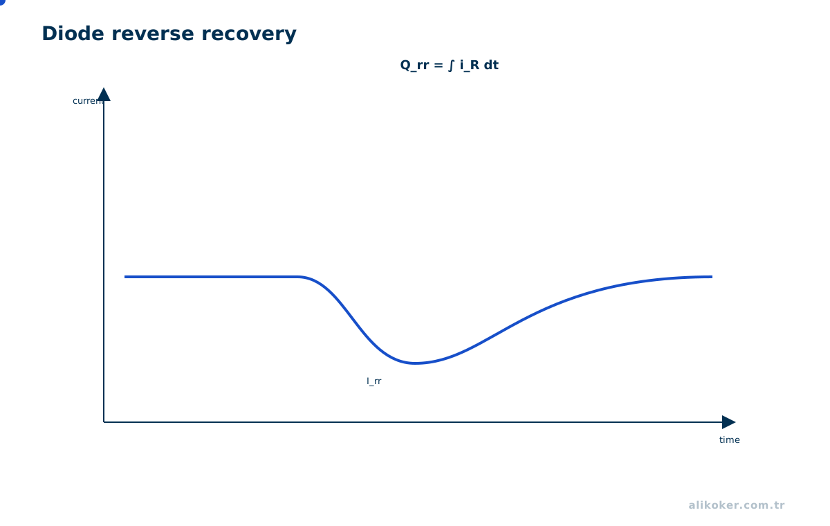
A power diode is not an ideal one-way switch. Forward voltage, reverse leakage, junction temperature, reverse recovery, and parasitic capacitance affect switching behavior.
Schottky devices can offer low forward drop and low reverse-recovery charge, but reverse-voltage capability, leakage, and high-temperature behavior may become limiting.
Selection must consider peak and RMS current, reverse voltage, thermal resistance, transients, and switching frequency rather than average current alone.
Recovery behavior matters as much as forward drop
Forward voltage determines conduction loss. Schottky diodes can provide low forward drop and very low reverse recovery, while reverse-voltage rating, leakage, and temperature limits remain application dependent. Fast PN diodes can create recovery current that increases switch stress and EMI.
Selection for a buck converter or motor freewheel path includes average, RMS, and peak current, reverse voltage, junction temperature, and recovery behavior. A package current rating is not automatically a safe continuous current without the specified copper area and thermal conditions.
Unit 3: BJT, MOSFET, and IGBT as Power Switches
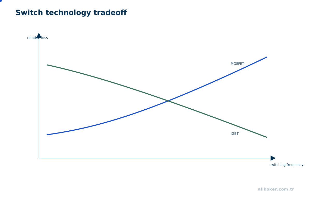
BJTs are current-driven devices, while MOSFETs and IGBTs are gate-driven power switches. The appropriate device depends on voltage, current, frequency, loss, and drive requirements.
A frequent MOSFET error is to interpret V_(GS(th)) as the voltage for full enhancement. Threshold voltage only defines the onset of a small drain current. Low R_(DS(on)) must be checked at the gate voltage for which the manufacturer actually specifies it.
Therefore a device with a 2–4 V threshold is not automatically suitable for efficient 5 V gate drive.
Choose device technology for the operating region
MOSFET conduction loss at low voltage is often approximated by I_rms^2 R_DS(on). R_DS(on) increases with temperature and is specified at particular V_GS and junction conditions. V_GS(th) is only the low-current threshold where conduction begins; it is not the fully enhanced gate voltage.
IGBTs can be advantageous at higher voltage and moderate switching frequency, with conduction behavior different from a purely resistive MOSFET model. BJTs are less common in modern fast low-voltage switching because they require base current and store charge, but their saturation behavior remains important conceptually.
Device selection includes gate charge, switching energy, avalanche capability, body-diode behavior, short-circuit withstand, package inductance, and thermal impedance in addition to voltage and current ratings.
Unit 4: Gate Drive and Gate Charge
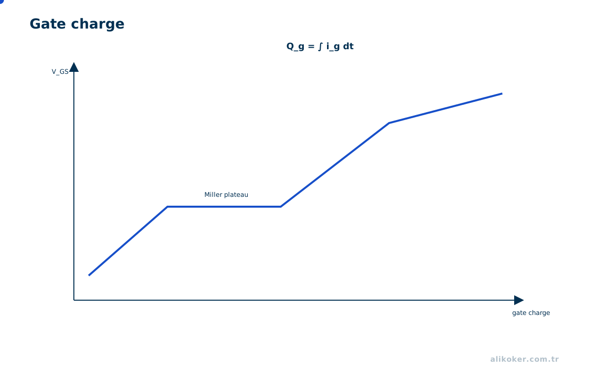
A MOSFET gate draws little DC current in steady state, but its capacitances must be charged and discharged during every transition. Approximate average gate-drive power scales as:
P_g ≈ Q_g V_g f_sGate resistance influences transition speed, ringing, and driver peak current. Excessive resistance increases transition loss; too little resistance can aggravate parasitic oscillation and EMI.
A gate-source pull-down prevents an unpowered or high-impedance driver from leaving the gate floating. At substantial current or frequency, a dedicated gate driver may be preferable to direct drive from a timer or MCU pin.
The gate is a dynamic load
A MOSFET gate draws little DC current but transfers gate charge during every switching event. Average driver power scales approximately as:
P_gate ≈ Q_g * V_drive * f_swGate resistance and driver source/sink current set transition speed. Slow edges increase switching loss; excessively fast edges increase dv/dt, di/dt, ringing, and EMI.
The Miller plateau occurs while drain voltage changes and gate voltage temporarily changes slowly. A high-side N-channel MOSFET requires gate voltage above the switching source node, using bootstrap, charge-pump, or isolated drive according to topology. Bootstrap drive has refresh constraints at very high duty ratio or low switching activity.
Unit 5: Conduction and Switching Losses
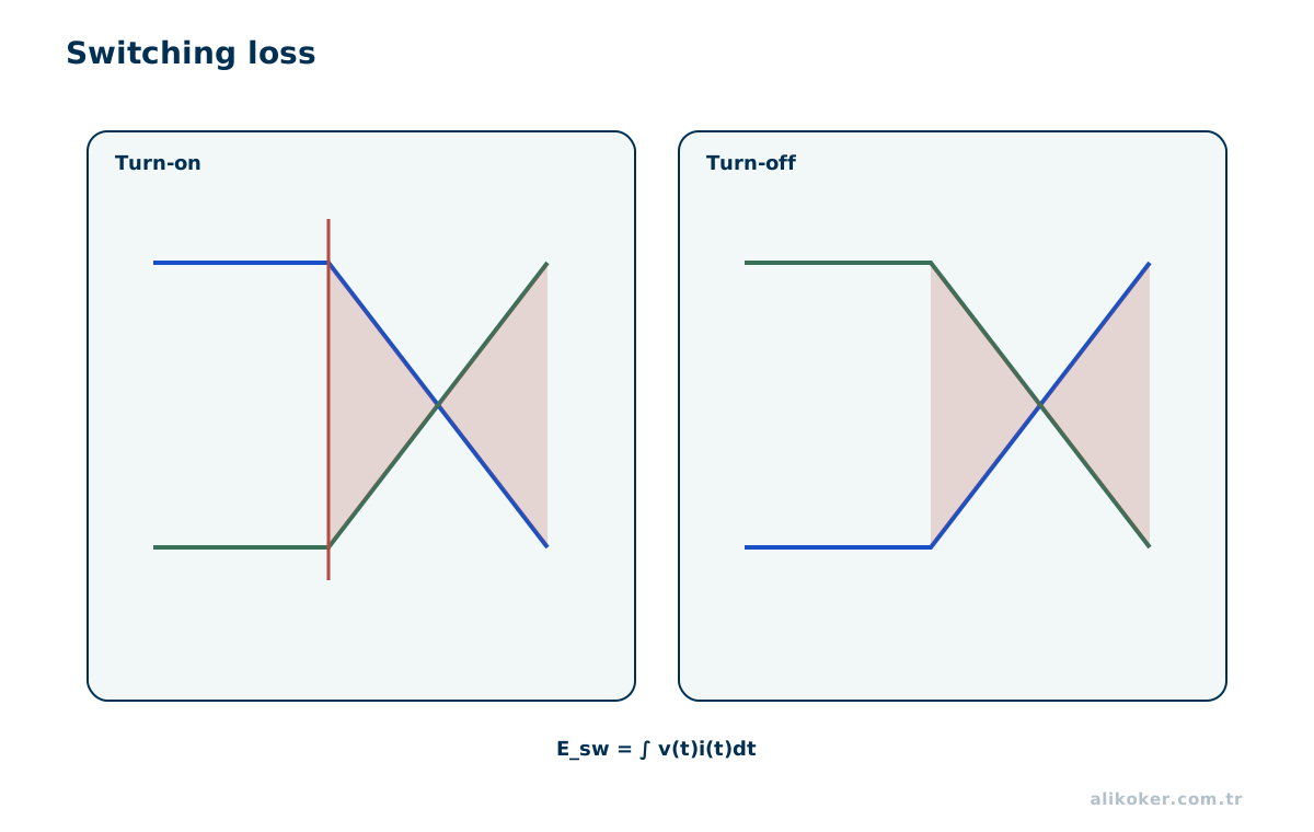
Approximate MOSFET conduction loss is:
P_cond≈ I_RMS^2R_(DS(on))and R_(DS(on)) normally increases with junction temperature.
Switching loss occurs because voltage and current overlap during finite transitions. A simplified scaling is:
P_sw∝ V I (t_r+t_f) f_sHigher frequency can improve filter size or acoustic behavior but generally increases switching loss, gate-drive loss, and EMI. Higher frequency is therefore not automatically better.
Calculate loss from the waveform
A first MOSFET conduction estimate is:
P_cond ≈ I_rms^2 * R_DS(on,T)Switching loss arises while voltage and current overlap. A simplified linear-transition estimate is:
P_sw ≈ 0.5 * V * I * (t_r+t_f) * f_swwhile Coss, diode recovery, and parasitics add further loss.
Use actual RMS and peak waveforms rather than one nominal current. Duty ratio, load, and conduction mode redistribute loss among switches and diodes. The worst thermal point is not always maximum output power.
Unit 6: Safe Operating Area and Thermal Design
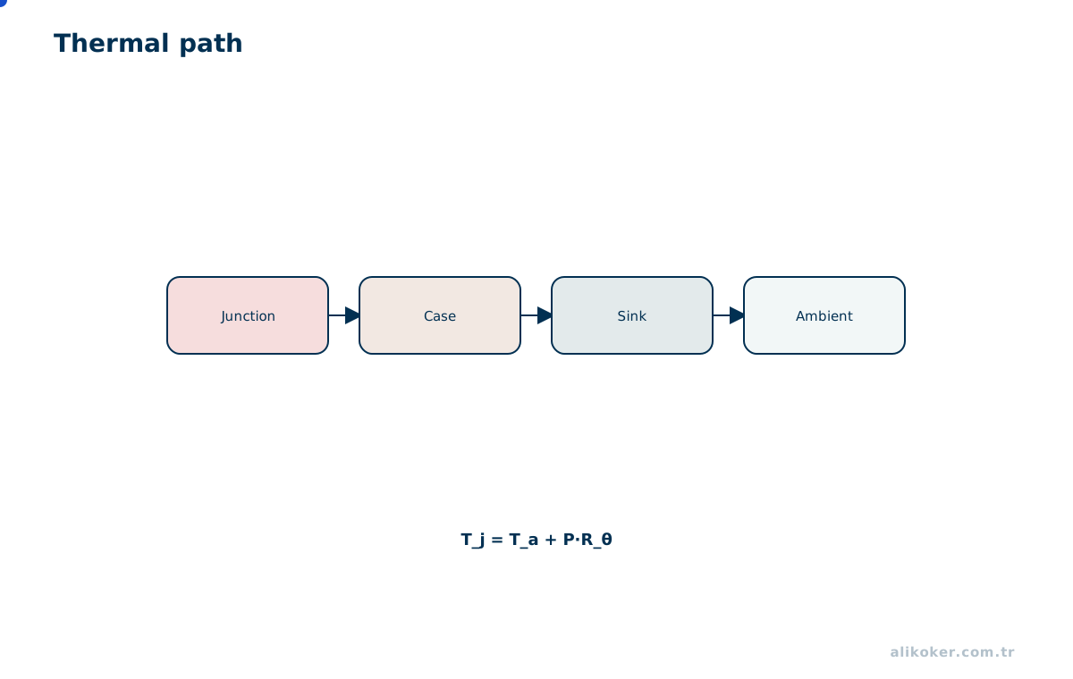
Current rating alone does not define a valid operating point. The Safe Operating Area constrains combinations of voltage, current, pulse duration, and temperature.
A simplified thermal model is:
T_j=T_a+P_lossθ_JAwhile PCB copper, package, airflow, heatsink, and interface materials determine the real thermal path.
Absolute maximum ratings are survival limits, not intended nominal operating points; engineering margin is required.
Electrical and thermal limits are coupled
A first junction-temperature estimate is:
T_j ≈ T_a + P_loss * R_θJAWith a heatsink, junction-to-case, interface, and sink-to-ambient paths are treated separately. Pulsed loading may require transient thermal-impedance curves rather than one steady thermal resistance.
Safe Operating Area defines permissible voltage-current-time combinations. A MOSFET's absolute maximum drain current cannot be assumed safe simultaneously with high V_DS. Linear mode and short-circuit stress require their own SOA analysis.
Unit 7: Parasitic Inductance, dv/dt, and di/dt
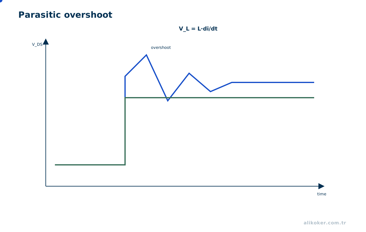
Rapid current change through parasitic inductance produces:
V=L(di)/(dt)voltage overshoot. The relevant inductance may be in PCB traces, wires, connectors, and package leads as well as intentional inductors.
High-di/dt current loops should be short and separated from low-level control and measurement paths. Ringing should be diagnosed before applying arbitrary damping components.
Layout is an electrical component
Only a few nanohenries in a switching loop can create meaningful overshoot at high di/dt:
V_L = L * di/dtThe high-frequency loop among DC-link capacitor, half-bridge switches, and freewheel path should therefore be physically short. Long wires and breadboards become unmodeled inductors in fast power circuits.
Drain ringing can exceed V_DS limits and increase EMI. Gate and power loops should be separated, Kelvin source connections used when available, and probe ground loops minimized because measurement wiring itself can modify the observed ringing.
Unit 8: Inductive Loads and Freewheeling Paths
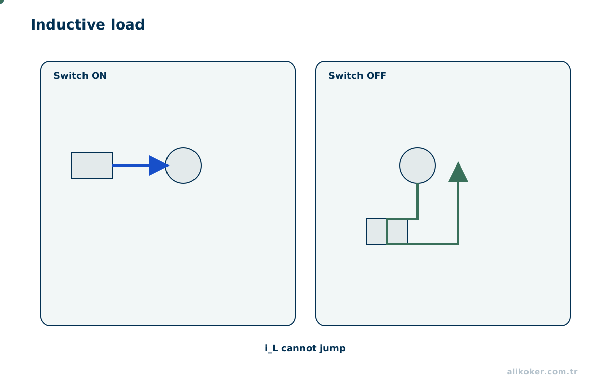
Inductor current cannot change instantaneously. When a switch driving a motor, solenoid, or relay opens, the stored magnetic energy requires a current path; otherwise a high transient voltage can appear across the switch.
A flyback diode is the simplest low-side DC solution. It is reverse-biased during normal energization and conducts the inductive current after turn-off.
For applications requiring fast release, a simple diode may decay current too slowly. TVS, Zener, or active clamps can permit a higher controlled voltage and faster energy dissipation. Protection topology must therefore match load dynamics.
Current continuity forces an energy path
An inductor stores E=0.5 L I^2, and current cannot become zero instantaneously. Without an alternate path after turn-off, voltage rises until some path conducts. A flyback or freewheel path provides controlled current decay for motors and solenoids.
A simple diode clamps voltage low and therefore releases current slowly. Solenoids that require faster release may use a zener, TVS, or active clamp, accepting higher voltage for faster current decay. Protection is therefore a current-decay design, not merely the presence of a diode.
Unit 9: NE555 PWM and the Transition to a Power Switch
The astable and monostable behavior of the NE555 belongs to Electronics I and II. In power electronics, the concern is how the resulting logic waveform safely controls the power device.
A timer-MOSFET-motor chain is:
NE555
 -> gate drive
 -> MOSFET
 -> motor
 -> flyback current path
 -> supply return path
For non-logic-level devices such as the IRFZ44N, adequate gate voltage is important. A series gate resistor and gate-source pull-down are common provisions for controlled switching and defined startup state. Motor startup/stall current must be checked against switch and flyback-device limits.
Separate timing from power conversion
An NE555 can generate PWM or clock waveforms, but it is not the element intended to carry motor current. The control waveform drives a gate driver or suitable MOSFET. Devices such as IRFZ44N may have a threshold of only a few volts but require substantially higher gate voltage for low R_DS(on); 5 V logic drive should not be assumed sufficient from threshold alone.
A series gate resistor controls peak driver current and switching speed, while a gate-source pull-down prevents an uncontrolled floating gate at startup. When the timer and motor share a supply, bypassing and return-current layout help prevent motor transients from false-triggering the control circuit.
The NE555 timing network belongs to Electronics I and II; MOSFET loss and motor current paths belong here.
Unit 10: PWM Duty Cycle and Frequency
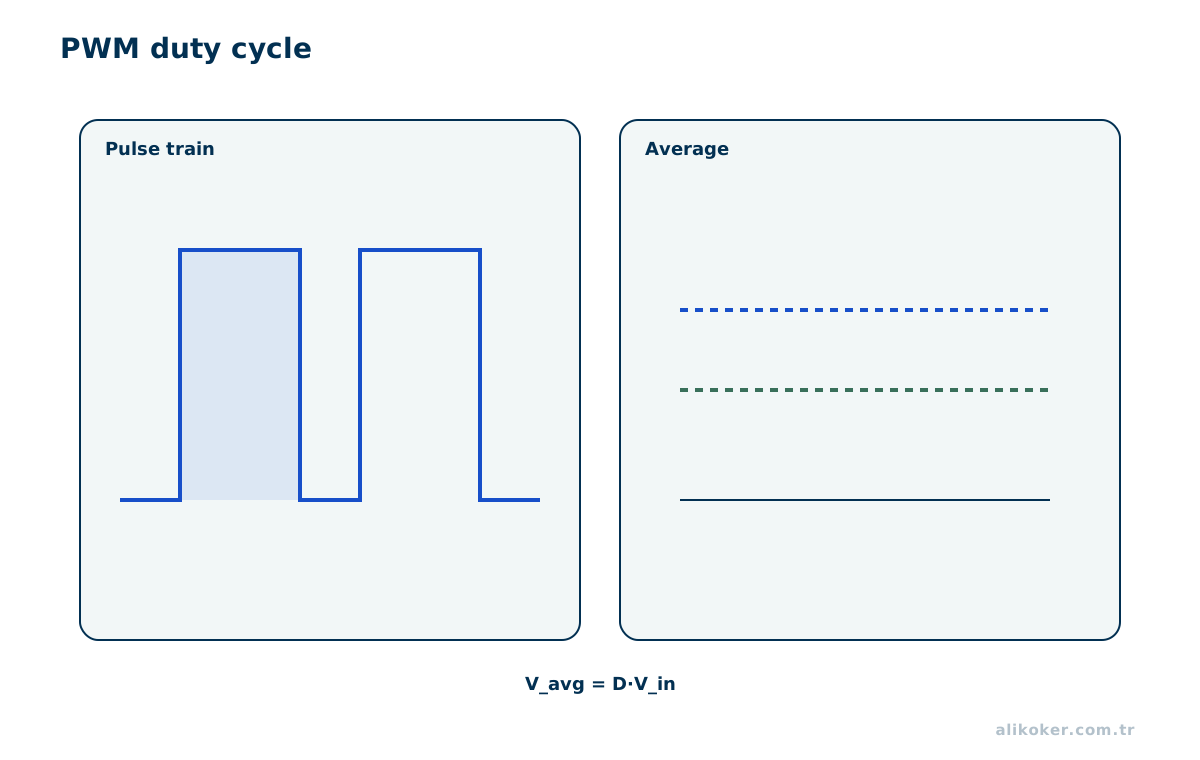
Duty cycle is:
D=(t_on)/(T)In an ideal buck-like average model:
V_avg≈ D V_inbut actual motor speed is not numerically equal to D; inductance, back EMF, load torque, supply impedance, and control architecture determine the operating point.
Very low PWM frequency may produce audible or mechanical ripple, while very high frequency increases switching loss. Acoustic behavior, current ripple, switch loss, driver capability, and EMI must be balanced.
Frequency selection is a multi-objective tradeoff
Duty cycle D=t_on/T describes the on-time fraction. In an ideal buck-like stage, average output can scale with D, while a motor's current, back EMF, and mechanical time constants alter the real response.
Increasing switching frequency can reduce ripple and magnetic size but increases switching and gate-drive loss. Low frequency can create large current ripple and audible components. Frequency is selected from semiconductor loss, inductance, EMI, control bandwidth, and acoustic constraints.
Unit 11: Rectifiers
Single-phase half-wave, full-wave, and bridge rectifiers convert AC to unidirectional voltage. Current waveform changes substantially between resistive and inductive loads.
A reservoir capacitor reduces output ripple but can create narrow high-peak diode currents. RMS and peak stresses therefore matter in addition to average DC load current.
Examine source and load waveforms together
A single-phase bridge with a capacitor-input filter produces smoother DC but can draw high current pulses near AC voltage peaks. This affects RMS current, diode peak stress, harmonics, and power factor.
Inductive loads can sustain current beyond voltage zero crossing and may require freewheeling paths. Three-phase rectifiers provide lower ripple and higher power capability. Design includes average DC output, PIV, RMS/peak current, ripple, inrush, and source impedance.
Unit 12: Phase-Controlled AC Power
SCRs and triacs can control load power by changing conduction angle. Inductive loads differ from resistive loads because current zero crossing and voltage zero crossing are not generally coincident.
Phase control introduces harmonics and can reduce power factor. Triggering and commutation for a motor load therefore differ from those of a heater.
Firing angle changes the waveform
SCR or triac phase control starts conduction at a selected angle in each half cycle. A resistive load current reaches zero with voltage, while an inductive load can continue after the voltage zero crossing. Conduction and commutation therefore depend on load phase.
Phase control is simple and robust but generates harmonics and can degrade EMI and power factor. It remains useful for heaters and some motor loads, while other topologies are preferred when power quality is critical.
Unit 13: Buck Converter
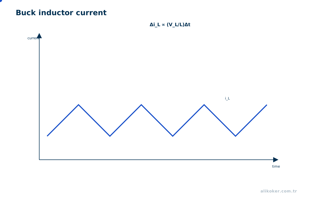
For an ideal buck converter in continuous conduction:
V_o=D V_inThe inductor stores energy while the switch is on and continues current through a diode or synchronous switch when it is off. Inductor-current ripple, capacitor ripple, ESR, and switching frequency determine output quality.
A module's advertised maximum current does not imply that the same continuous current is safe for every input/output ratio and thermal environment.
Energy moves through two switching intervals
When the buck switch is on, the inductor sees energy from the source and current rises; when the switch is off, current continues through the freewheel path. In ideal continuous-conduction mode:
V_out ≈ D * V_inInductor ripple follows operating point, L, and switching frequency.
CCM and DCM are not identical. At light load, inductor current can reach zero and the conversion ratio becomes load dependent. Output capacitance and ESR determine output ripple, while the input capacitor supplies local pulsed switch current.
Unit 14: Boost Converter
For an ideal CCM boost converter:
V_o=(V_in)/(1-D)As duty approaches one, the ideal equation tends toward an unbounded output, but real systems are constrained by switch and diode loss, inductor resistance, current limit, and control stability.
Because a conventional boost topology retains an input-to-output path through the diode, complete load disconnect may require additional circuitry.
Energy is first stored, then added to the input
With the switch on, the boost inductor stores energy; when off, inductor voltage adds to the input and transfers energy to the output. Ideal CCM gives:
V_out ≈ V_in / (1-D)The ideal expression appears unbounded as D approaches one, but real loss, peak current, and control limits prevent this.
Boost input current is often continuous, while switch and diode see higher voltage stress. The diode path from input to output can also influence startup, precharge, and shutdown behavior.
Unit 15: Buck-Boost and Isolated Converters
Buck-boost families can produce output below or above the input. When galvanic isolation is required, flyback, forward, push-pull, half-bridge, and full-bridge transformer topologies may be used.
Isolation is not achieved merely by adding a transformer. Creepage and clearance, insulation system, feedback isolation, Y capacitors, and applicable safety requirements are part of the design.
Topology choice is more than voltage ratio
An inverting buck-boost reverses polarity, while SEPIC and non-inverting buck-boost structures can regulate above and below the input. Isolated topologies add a transformer for safety, grounding separation, or large conversion ratio.
Flyback stores energy in magnetizing inductance and transfers it after switch turn-off; forward and bridge converters transfer energy differently. Flux reset, leakage inductance, and isolation spacing are physical design constraints.
Unit 16: Inverters and H-Bridges
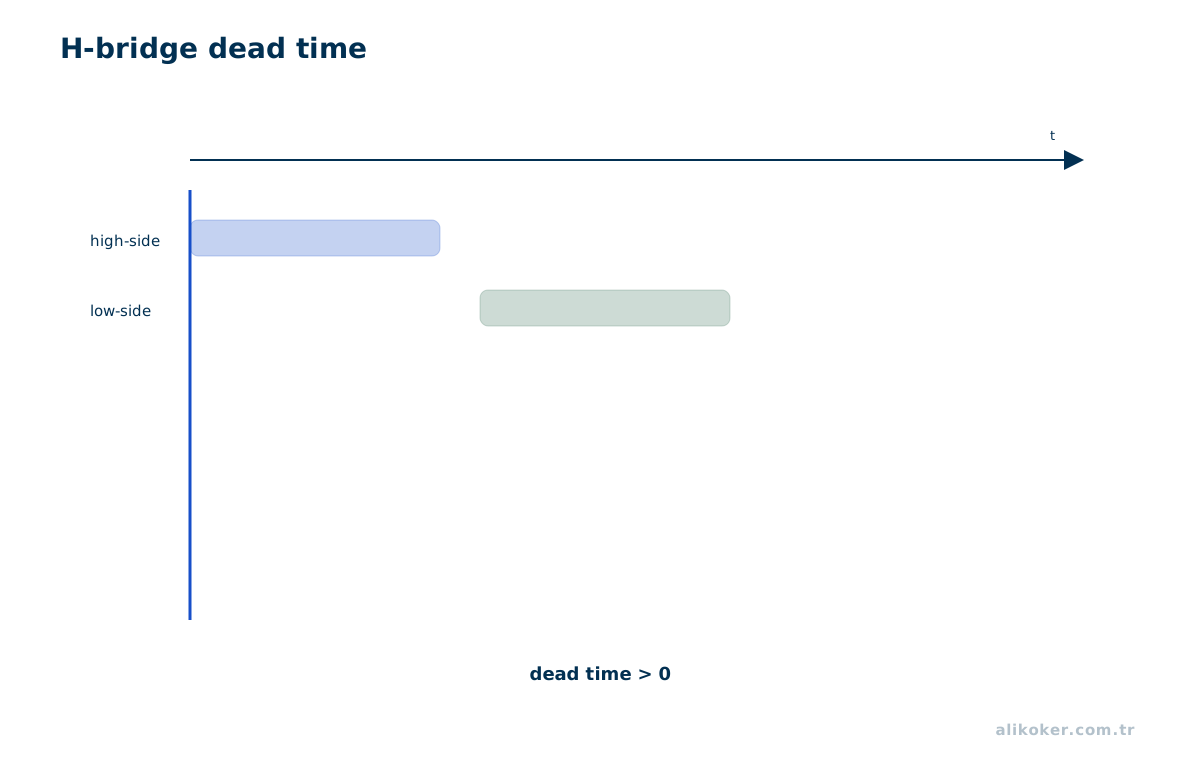
An H-bridge uses four switches to reverse load voltage. It can drive a DC motor bidirectionally or synthesize AC-like waveforms from a DC source.
If the high-side and low-side devices of the same leg conduct simultaneously, shoot-through occurs. Dead time prevents that condition, but excessive dead time distorts current and torque.
Driving a high-side N-channel MOSFET differs from low-side drive because its source node moves with the switching waveform.
Simultaneous conduction creates shoot-through
An H-bridge applies both polarities of a DC bus to a load. Turning on the high-side and low-side device of one leg simultaneously shorts the bus. Gate-driver dead time reduces this risk, although excessive dead time distorts output voltage and can increase torque ripple.
Inductive motor current continues after switch transitions through body diodes or synchronous MOSFET paths. Under regeneration, energy can flow back to the DC bus, which must be able to absorb it.
Unit 17: Sinusoidal PWM and Multiphase Inverters
Sinusoidal PWM compares a sinusoidal reference with a carrier waveform to produce switching commands. Modulation ratio affects the fundamental output component.
Three-phase inverters drive induction, PMSM, and BLDC machines. Advanced voltage-vector and current-control strategies belong to motor-control specialization; this course focuses on the power stage and energy paths.
Modulation controls fundamental and harmonics
Sinusoidal PWM compares a sinusoidal reference with a triangular carrier. Modulation index affects fundamental amplitude, while carrier ratio shapes harmonic distribution. In multiphase inverters, phase timing and dead-time symmetry influence current balance.
Motor drives care about phase-current waveform and DC-link ripple as well as phase voltage. Space-vector methods can use the DC bus differently, but the core safety requirement remains correct switch-state sequencing and current paths.
Unit 18: Static Switches and Solid-State Relays
Solid-state relays use semiconductors instead of mechanical contacts. DC implementations may use MOSFETs, while AC versions can use triacs, SCRs, or back-to-back MOSFET structures.
An SSR does not provide zero leakage when off or zero voltage drop when on. Thermal loss, leakage current, dv/dt immunity, and isolation rating are selection criteria.
Isolation and leakage behavior
An SSR removes mechanical contact wear but does not provide zero off-state leakage or zero on-state drop. AC SSRs are often triac/SCR based and may include zero-cross turn-on; DC SSRs may use MOSFETs.
Optical isolation separates control and power domains, while creepage, clearance, dv/dt immunity, and isolator lifetime still require design. Semiconductor failures may become short circuits, so the safe-state assumption should not simply be “SSR fails open.”
Unit 19: Switched-Mode Power Supplies
An SMPS combines switching and energy-storage components for efficient regulation. Design includes not only topology but also control-loop behavior, magnetics, input/output filters, transient response, EMI, isolation, thermal design, and protection.
Source and load cannot always be designed independently. Pulsed or motor loads can interact with converter current limits, control loops, and input-source impedance.
Regulation is more than producing PWM
An SMPS includes sensing, error processing, compensation, startup, soft-start, and protection in addition to the power stage. The control loop is designed around converter plant dynamics.
Output capacitor ESR/ESL, inductor tolerance, and source impedance influence loop behavior. An EMI input filter adds its own dynamics and can interact with the converter if poorly damped. Power and control design are therefore coupled.
Unit 20: Motor Interaction with DC-DC Converters
A motor can draw startup or stall current far above normal running current. The nominal current printed on a buck module does not guarantee survival of that transient.
Failures involving an LM2596-class regulator and a DC motor illustrate a general engineering chain:
motor load
 -> startup current
 -> switching transient
 -> capacitor ESR/ESL
 -> converter current limit
 -> thermal and SOA limits
A fuse can reduce fire risk from sustained overcurrent, but it is not a substitute for fast transient suppression. Correct freewheeling, clamps, snubbers, and an appropriately rated power stage are separate requirements.
A motor is not a constant resistor
DC motor current depends dynamically on speed and torque. At startup, low back EMF creates high current demand; during braking or load release, energy flow can reverse. A buck module such as an LM2596-based board cannot be selected for motor service from its headline current rating alone.
Input wiring inductance, converter current limit, output capacitance, and motor transients should be analyzed together and verified during startup and stall tests. Peak/current-limit behavior can differ substantially from continuous-current ratings.
Unit 21: Bypass, Ground, and Current Loops
Routing high-current switching return through the same impedance used by sensitive control circuitry can cause ground bounce and false triggering. Power-current loops should be short and low impedance, with control references arranged deliberately.
Small ceramic capacitors support fast local current transients while larger bulk capacitors support slower energy demand. One large electrolytic capacitor is not a substitute for high-frequency bypassing.
Brush-motor EMI can also be reduced through suitable terminal suppression and short or twisted motor wiring.
Placement matters as much as capacitance value
High-frequency switching current should not travel through long traces to a remote bulk capacitor. Ceramic bypass capacitors belong physically close to the switching loop, while bulk capacitance supports lower-frequency energy demand. ESR and ESL determine real transient behavior.
If power current shares uncontrolled impedance with sensitive signal return, ground bounce results. “Star ground” can help in some low-frequency systems, while high-frequency PCB design focuses on continuous low-impedance return planes and controlled loop geometry.
Unit 22: Protection
Power-stage protection may require several complementary functions:
- overcurrent / short-circuit protection,
- reverse-polarity protection,
- overvoltage,
- undervoltage,
- overtemperature,
- inrush control,
- transient suppression,
- shoot-through prevention,
- gate-overvoltage protection.
Threshold and response time must be matched to the electrical and thermal survivability of the protected component.
Protection layers target different time scales
A fuse is important for wiring and fire protection but may be too slow to protect a MOSFET from microsecond-scale stress. Cycle-by-cycle current limiting, desaturation or OCP comparators, TVS devices, snubbers, thermal shutdown, and fuses address different faults and time scales.
Reverse polarity, load dump, ESD/EFT, short circuit, and open-load conditions are application dependent. Protection also changes normal losses and parasitics; a series diode is simple but lossy, while an ideal-diode MOSFET reduces loss at the cost of added control complexity.
Unit 23: Measurement and Laboratory Safety
An oscilloscope ground clip may be connected to protective earth. Connecting it incorrectly to a mains-referenced or floating switching node can create a short circuit and shock hazard.
Initial bring-up with a current-limited laboratory supply and low available energy can reduce damage from wiring errors and unintended gate states. Breadboards are inappropriate for substantial motor current because contact resistance and heating become uncontrolled.
Capacitors retain energy after power removal:
E=(1)/(2)CV^2so discharge and verification procedures are part of safe testing.
Know the instrument topology before connecting a probe
The ground clip of many bench oscilloscopes is bonded to protective earth. Connecting it incorrectly to a line-referenced or floating high-side node can create a short circuit and shock hazard. Differential high-voltage probes, isolated measurement, or current probes should be chosen from the actual circuit topology.
Initial energization can use current-limited supplies, appropriate series limiting or protection, low duty cycle, and thermal observation. Large DC-link capacitors can retain hazardous energy after power removal; discharge paths and verification measurements belong to the procedure.
Unit 24: Power-Stage Design Workflow
A robust design sequence is:
input/output requirement
 -> normal and peak load
 -> topology
 -> switch/diode voltage-current margin
 -> gate drive
 -> magnetic and capacitive components
 -> loss and thermal analysis
 -> transient protection
 -> PCB current loops
 -> low-energy bring-up
 -> real-load validation
Simulation is useful but cannot fully substitute for measurement of parasitics, thermal interfaces, connectors, and transient behavior of real loads such as motors.
Design checklist
A practical sequence is:
input/output limits
-> nominal and transient load
-> topology
-> switch/diode stress
-> magnetic and capacitive energy storage
-> gate drive
-> conduction/switching loss
-> junction temperature
-> protection
-> layout/current loops
-> measurement
-> worst-case validation
The calculation should cover minimum and maximum input, temperature, tolerance, startup, stall, short circuit, and load steps. Prototype waveforms are then compared with the model to verify overshoot, ringing, ripple, and thermal equilibrium.
Course Boundaries
The internal comparator/latch/timing structure of the NE555 belongs to Electronics I and II; Fourier and sampling aspects of PWM to Signals and Systems; timer peripherals to Microprocessors; motor torque-speed and electromechanical models to Actuators, Electrical Machines and Drive Systems; and speed/position control to Automatic Control. This course owns the power-conversion layer between them.
Design Example: PWM Brushed-DC Motor Power Stage
A low-side motor switch exposes the main decisions of power electronics in a compact circuit. Start with stall current, supply voltage, wiring, and connector limits. Select MOSFET V_DS with transient margin, evaluate R_DS(on) at actual gate voltage and temperature, and interpret current ratings under pulse and thermal constraints.
PWM source
 -> gate driver / series gate resistor
 -> N-MOSFET
 -> motor
 -> freewheel diode or synchronous path
 -> DC bus
When the MOSFET turns off, motor current transfers to the freewheel path. Diode peak/RMS current and reverse-voltage ratings must match that current. MOSFET conduction loss, switching loss, and diode loss are converted into junction temperature. Inadequate gate drive can leave the MOSFET partially enhanced and increase conduction loss.
Long breadboard jumpers add parasitic inductance to the power loop, creating overshoot and ringing. Appropriate bulk capacitance, low-ESL local bypass, motor EMI suppression, and controlled current returns are part of the circuit. Even oscilloscope probe grounding can alter the observed transient.
Initial testing can use a current-limited supply, low duty cycle, and thermal observation before progressing to stall, load-step, and sustained-temperature tests. The PWM source may be an NE555, MCU, or another controller; the energy and safety principles of the power stage remain the same.
References
- Erickson, R. W.; Maksimović, D. Fundamentals of Power Electronics. Springer, 2001.
- Gürdal, O. Güç Elektroniği. Bursa Orhangazi University Press, 2015.
- Mohan, N.; Undeland, T. M.; Robbins, W. P. Power Electronics: Converters, Applications, and Design. Wiley, 2003.
