Electronics I and II: Analog and Digital Circuit Fundamentals

Electronics I-II course notes covering circuit laws, semiconductors, diode and transistor circuits, amplifiers, operational amplifiers, filters and digital electronics.
The material is organized around the physical relationships that determine circuit behavior rather than around memorized formulas. The sequence runs from Ohm's and Kirchhoff's laws through semiconductor devices, transistor biasing, amplifiers, and the transition to digital electronics. Sign conventions, operating regions, and ideal-model assumptions are kept explicit because mixing these levels is a common source of error in elementary circuit analysis.
Unit 1: Fundamental Electrical Quantities and Circuit Elements
Electric charge
Electric charge is a basic physical quantity measured in coulombs. The elementary charge magnitude is approximately:
e = 1.602 x 10^-19 CCurrent in conductors can be understood as the rate of charge transfer, while electrostatic behavior depends on the distribution of charge and the resulting field.
Electric field
Electric field is force per unit positive test charge:
E = F / qIt is a vector. In circuit theory the field is usually not solved directly; lumped voltage and current variables provide a simpler model when physical dimensions and signal frequencies justify the lumped-element approximation.
Potential difference
Voltage is energy per unit charge:
V = W / qA voltage is always a difference between two points. A circuit chooses a reference node so other node voltages can be expressed relative to it.
Electric current
Current is the time rate of charge flow:
i(t) = dq/dtConventional current direction is defined as positive-charge flow. Electron drift in metals is opposite to conventional current.
Energy and power
Electrical power is:
p(t) = v(t) i(t)Under the passive sign convention, positive power means the element absorbs energy and negative power means it delivers energy.
For constant values:
W = P tconnects power and transferred energy.
Resistance and Ohm's law
For an ideal linear resistor:
v = i Rand therefore:
P = VI = I^2 R = V^2 / Rwhere the equivalent forms follow from Ohm's law.
Ohmic and non-ohmic elements
An ohmic element has an approximately linear v-i relation over the operating range being considered. Semiconductor junctions, lamps over large temperature ranges and many other devices are nonlinear; a constant resistance is not a complete model for them.
Temperature dependence
For a limited temperature interval, resistance is often approximated as:
R(T) = R0 [1 + alpha (T - T0)]The coefficient depends on material and the approximation range. Semiconductor temperature behavior can be very different from a metal resistor's positive coefficient.
Inductor
An ideal inductor relates voltage to current change:
v(t) = L di/dtand stores magnetic-field energy:
W = 1/2 L i^2Ideal inductor current cannot change discontinuously without infinite voltage. Real inductors add winding resistance, parasitic capacitance, core loss and saturation limits.
Capacitor
An ideal capacitor follows:
i(t) = C dv/dtand stores electric-field energy:
W = 1/2 C v^2Ideal capacitor voltage cannot change discontinuously without infinite current. Real capacitors have ESR, leakage, dielectric loss and voltage/frequency limits.
Ideal sources
An ideal voltage source maintains its specified voltage regardless of current; an ideal current source maintains its specified current regardless of voltage. These are analysis models. Real sources have finite voltage/current compliance and internal impedance.
Unit 2: DC Circuits and Circuit Analysis
Electromotive force
A source converts non-electrical energy into electrical potential difference. The historical term electromotive force is measured in volts even though it is not a mechanical force.
Maximum power transfer
For a Thevenin source with resistance Rth, a purely resistive load receives maximum power when:
RL = RthThe theorem concerns maximum delivered load power, not maximum efficiency. At the matching point in the simple DC-resistive model, source resistance dissipates the same power as the load.
Series and parallel resistors
Series resistors carry the same current:
Req = R1 + R2 + ...Parallel resistors share the same voltage:
1/Req = 1/R1 + 1/R2 + ...For two resistors:
Req = R1 R2 / (R1 + R2)Kirchhoff's current law
KCL follows charge conservation. At a node, the algebraic sum of branch currents is zero:
sum i_k = 0A consistent sign convention is enough; currents assumed in the wrong physical direction simply solve to negative values.
Kirchhoff's voltage law
KVL states that the algebraic sum of voltages around a closed lumped circuit path is zero:
sum v_k = 0This is consistent with energy conservation under the assumptions of ordinary lumped circuit theory.
Nodal analysis
Nodal analysis chooses a reference node, assigns unknown node voltages and applies KCL. Branch currents are written in terms of voltage differences and element relations.
For a resistor between nodes a and b:
i_ab = (Va - Vb) / RThe resulting simultaneous equations determine node voltages.
Mesh analysis
Mesh-current analysis assigns loop currents to independent meshes in a planar circuit and applies KVL. Shared elements contain the algebraic difference of adjacent mesh currents.
Nodal analysis is often more direct for circuits with many current sources; mesh analysis can be convenient for voltage-source-dominated planar circuits.
Voltage divider
For two series resistors:
Vout = Vin R2 / (R1 + R2)provided the output is unloaded or the load has already been incorporated into the equivalent resistance. Connecting a load changes the divider ratio.
Current divider
For two parallel resistors carrying total current I:
I1 = I R2 / (R1 + R2)
I2 = I R1 / (R1 + R2)
The lower-resistance branch carries more current.
Thevenin equivalent
A linear two-terminal network can be represented at its port as an ideal voltage source Vth in series with Rth or, for AC linear networks, impedance Zth.
Vth is the open-circuit terminal voltage. The equivalent resistance can be found by suppressing independent sources and looking into the port, or with test-source methods when dependent sources are present.
Norton equivalent
The same linear network can be represented by a current source In in parallel with Rn:
Rn = Rth
In = Vth / Rth
for the ordinary non-degenerate resistive case.
Source transformation
A voltage source V in series with R is equivalent at its terminals to a current source I = V/R in parallel with the same resistance. The equivalence concerns terminal behavior, not internal element currents in the original network.
Unit 3: AC Circuits, Phasors and Frequency Behavior
Sinusoidal signals
A sinusoid can be written:
v(t) = Vm sin(omega t + phi)with amplitude Vm, angular frequency omega = 2 pi f, frequency f, and phase phi.
RMS value
For a sine wave:
Vrms = Vm / sqrt(2)
Irms = Im / sqrt(2)
RMS gives the DC-equivalent heating effect in a resistor.
Phasors
For linear steady-state sinusoidal analysis, a sinusoid can be represented by a complex phasor. Differentiation becomes multiplication by j omega and integration division by j omega, converting differential equations into algebraic impedance relations.
Resistor, inductor and capacitor in AC
Ideal resistor:
Z_R = RVoltage and current are in phase.
Ideal inductor:
Z_L = j omega LCurrent lags voltage by 90 degrees in the ideal sinusoidal steady-state model.
Ideal capacitor:
Z_C = 1 / (j omega C)Current leads voltage by 90 degrees.
Series RLC
For series RLC:
Z = R + j(omega L - 1/(omega C))At series resonance:
omega0 = 1 / sqrt(LC)the reactive terms cancel ideally and impedance is resistive.
AC power
Using RMS phasors, complex power is:
S = V I* = P + jQwhere P is real power, Q reactive power and |S| apparent power. Power factor is cos(phi) for sinusoidal single-frequency conditions.
RC filters
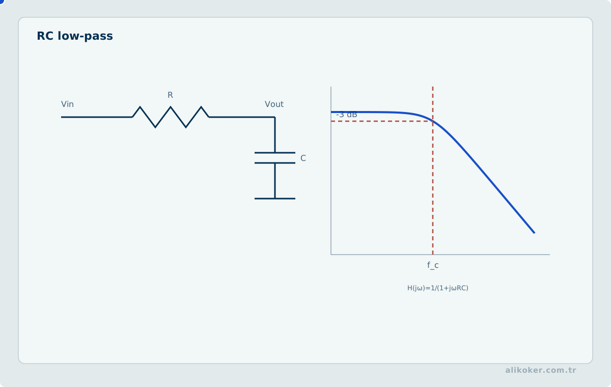
A first-order RC low-pass with output across the capacitor has:
H(jw) = 1 / (1 + jwRC)and cutoff:
fc = 1 / (2 pi RC)A first-order high-pass with output across the resistor has:
H(jw) = jwRC / (1 + jwRC)Under appropriate frequency/time-scale assumptions, RC networks can approximate differentiation or integration, but those approximations are valid only over a limited band.
Unit 4: Physical Foundations of Semiconductors
Energy bands
In solids, allowed electron energies form bands separated by forbidden regions. Electrical behavior depends strongly on band occupancy and band-gap size.
Conductors have readily available states for charge transport; insulators have large effective barriers; semiconductors have a moderate band gap that allows carrier concentration to be controlled by temperature, light and doping.
Electrons and holes
A missing electron in the valence-band bonding structure can be modeled as a positively charged mobile hole. Semiconductor current can therefore be described through electron and hole carriers.
Intrinsic semiconductor
A pure semiconductor has thermally generated electron-hole pairs. At equilibrium in an ideal intrinsic material, electron and hole concentrations are equal.
Doping
Adding donor impurities produces n-type material with electrons as majority carriers. Acceptor impurities produce p-type material with holes as majority carriers. The material remains electrically neutral on the macroscopic scale.
Fermi level
The Fermi level is an energy reference connected to carrier occupancy probability. Doping shifts its position relative to intrinsic material and the band edges. It should not be interpreted simply as a physical voltage source inside the semiconductor.
Temperature and light
Semiconductor conductivity generally changes strongly with carrier concentration and mobility. Temperature can increase intrinsic carrier generation, while illumination can generate additional electron-hole pairs. A photoresistor exploits conductivity change with light, though its material/device physics differs from a PN photodiode.
Unit 5: PN Junctions and Diodes
PN junction
When p-type and n-type regions form a junction, carrier diffusion leaves ionized dopants near the interface, creating a depletion region and built-in electric field. At equilibrium, diffusion and drift balance and net current is zero.
Forward and reverse bias
Forward bias reduces the effective barrier and allows significant carrier injection. Reverse bias increases the depletion field and only a small leakage current flows until breakdown mechanisms become important.
Diode equation
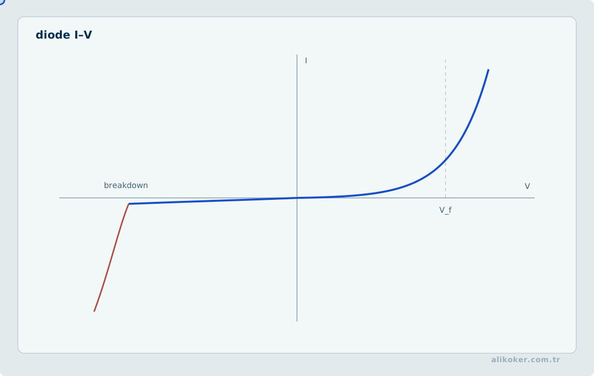
An idealized junction relation is:
I = Is [exp(Vd/(n Vt)) - 1]where Is is saturation current, Vt thermal voltage and n an ideality factor. Real devices add series resistance, leakage, recombination, capacitance and thermal effects.
Circuit models
Useful models include:
- ideal diode,
- constant-voltage-drop approximation,
- piecewise-linear model,
- exponential model.
The appropriate model depends on the required accuracy and operating region.
Load line
A diode/transistor circuit can be solved graphically by intersecting the nonlinear device characteristic with the external circuit's load line. The intersection is the operating point.
Rectifiers
A half-wave rectifier passes one half-cycle. A full-wave rectifier uses both half-cycles, commonly through a bridge or center-tapped topology.
A reservoir capacitor reduces output ripple by charging near waveform peaks and supplying the load between peaks. Ripple depends on load current, capacitance and line/rectified frequency; the capacitor does not produce perfectly constant DC.
Zener diode and breakdown
A reverse-biased junction can enter breakdown. Zener tunneling dominates at lower breakdown voltages and avalanche multiplication at higher ones, with a transition region where both contribute. A Zener diode is designed to operate safely in breakdown with current limiting.
Tunnel diode and LED
A tunnel diode uses heavy doping and quantum tunneling, producing a negative-differential-resistance region. An LED emits photons when electron-hole recombination releases energy in a suitable direct-band-gap semiconductor. LED current must be limited by the driving circuit.
Unit 6: BJT Transistors
Structure and currents
A BJT consists of emitter, base and collector regions in NPN or PNP form. Terminal currents satisfy:
IE = IC + IBIn the forward-active region a common approximate relation is:
IC ≈ beta IBbut beta varies with device, current, temperature and operating point and should not be treated as an exact circuit constant.
Operating regions
- cutoff: both junction conditions correspond to essentially off operation,
- forward active: used for amplification,
- saturation: both relevant junctions are forward biased and the transistor behaves as a strongly conducting switch rather than a linear current amplifier.
Common-base, common-emitter and common-collector
Common-emitter provides substantial voltage/current gain and phase inversion. Common-collector, or emitter follower, provides voltage near unity gain with useful impedance transformation. Common-base offers low input impedance and can be useful at high frequency.
Biasing
Bias establishes a quiescent point so the signal can vary without immediately clipping or leaving the intended operating region. Voltage-divider bias with emitter degeneration provides better stability than a simple fixed base-current bias because emitter feedback reduces sensitivity to transistor gain.
DC load line and Q point
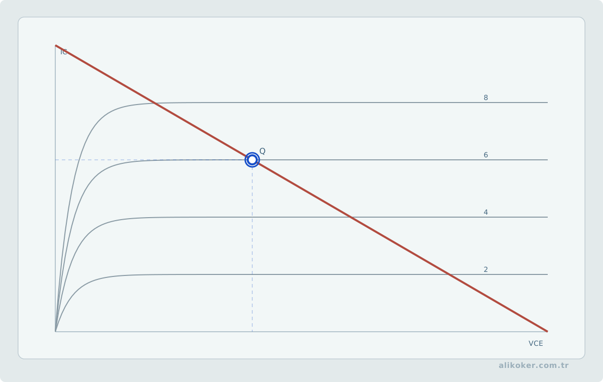
The external collector circuit imposes a relation such as:
VCE = VCC - IC RCfor the simplest common-emitter stage. The intersection with the transistor behavior determines the quiescent operating point Q.
Unit 7: FET and MOSFET
Field-effect transistor
A field-effect transistor controls channel current primarily through an electric field. It has high input impedance because the controlling gate ideally draws little steady-state current.
JFET
A JFET uses a reverse-biased gate junction to control channel width. In the usual n-channel model, increasingly negative VGS reduces drain current. The transfer characteristic is often approximated by Shockley's relation within the appropriate region:
ID = IDSS (1 - VGS/VP)^2with device-specific sign conventions.
Transconductance
Small-signal transconductance is:
gm = dID/dVGSat the operating point. It links a small gate-voltage change to drain-current change.
MOSFET
A MOSFET uses an insulated gate. Enhancement n-channel MOSFETs require gate-to-source voltage beyond threshold to form a strong inversion channel.
Basic regions are commonly described as:
- cutoff,
- triode/linear,
- saturation.
The word saturation does not mean the same device physics as BJT saturation. In a MOSFET, saturation is the region commonly used for analog current-source/amplifier operation, while the low-resistance linear region is used for an on-switch.
Bias point, small-signal model, and operating region
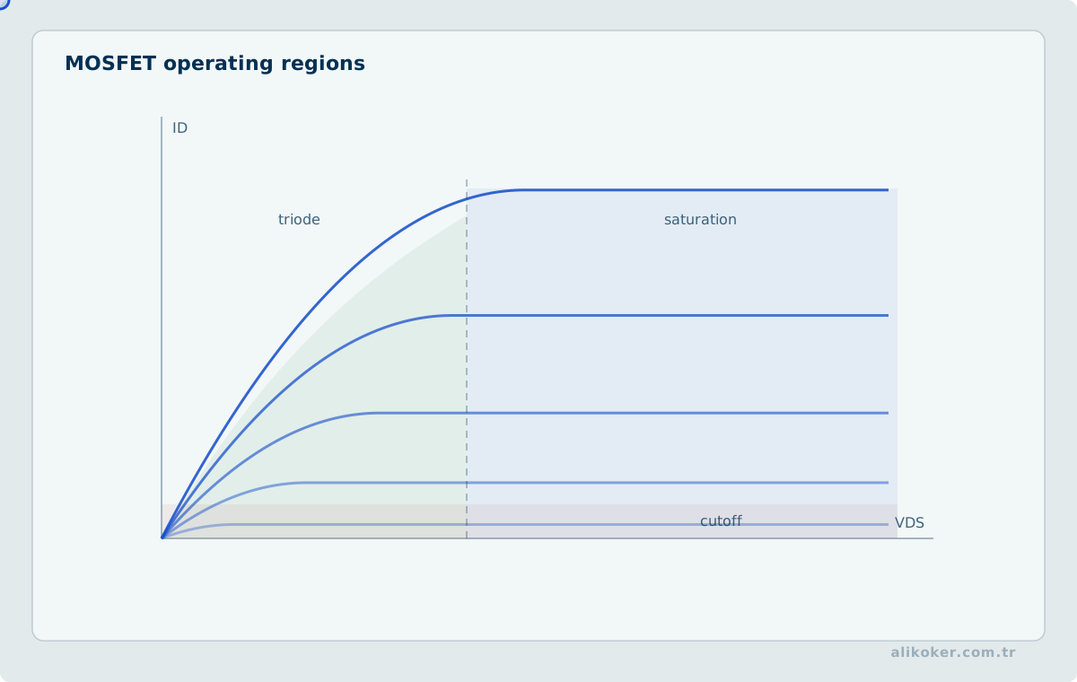
An amplifier must first establish a valid DC operating point. Small-signal analysis then linearizes the device around that point. Mixing the two views leads to incorrect gain and headroom estimates.
For a BJT, cutoff, forward-active, and saturation regions correspond to different junction biases. For a MOSFET, cutoff, triode, and saturation describe different relations among gate, drain, source, and threshold voltages.
The small-signal parameters are operating-point dependent. Gain therefore changes when bias current, load, temperature, or device parameters change.
Operational-amplifier nonidealities
The ideal op-amp model is useful, but real circuits are constrained by finite open-loop gain, gain-bandwidth product, slew rate, input offset, bias current, output-current limit, common-mode range, and output swing.
Negative feedback can control closed-loop gain only while the amplifier remains inside these limits. A mathematically valid resistor ratio can still produce saturation, slew-rate distortion, or instability in hardware.
Unit 8: Small-Signal Amplifiers and Operational Amplifiers
Amplifier concept
An amplifier uses energy from a supply to produce an output signal related to an input signal with controlled gain. Voltage, current, transconductance and power gain are different quantities.
Small-signal model
A nonlinear transistor can be linearized around a bias point for sufficiently small variations. The resulting incremental model allows AC gain and impedance to be analyzed with linear circuits while the DC bias is handled separately.
Common-emitter and common-base stages
A common-emitter BJT stage typically provides inverted voltage gain. Emitter resistance can stabilize gain and improve linearity at the cost of gain. Bypass capacitors can make the feedback frequency-dependent.
A common-base stage has low input impedance and no common-emitter phase inversion; its high-frequency behavior can be useful in some topologies.
Feedback
Negative feedback trades open-loop gain for controlled closed-loop gain, improved linearity, wider useful bandwidth and reduced sensitivity to parameter variation, provided the loop remains stable. Positive feedback is used deliberately in oscillators and hysteretic comparators but can destabilize an amplifier.
Operational amplifier
An ideal op-amp model assumes:
- infinite open-loop gain,
- infinite input impedance,
- zero output impedance,
- infinite bandwidth.
Real op-amps violate all of these assumptions. The ideal rules are valid only when the circuit is operating with negative feedback and the required output remains within input common-mode, output swing, slew-rate, current and stability limits.
Inverting amplifier
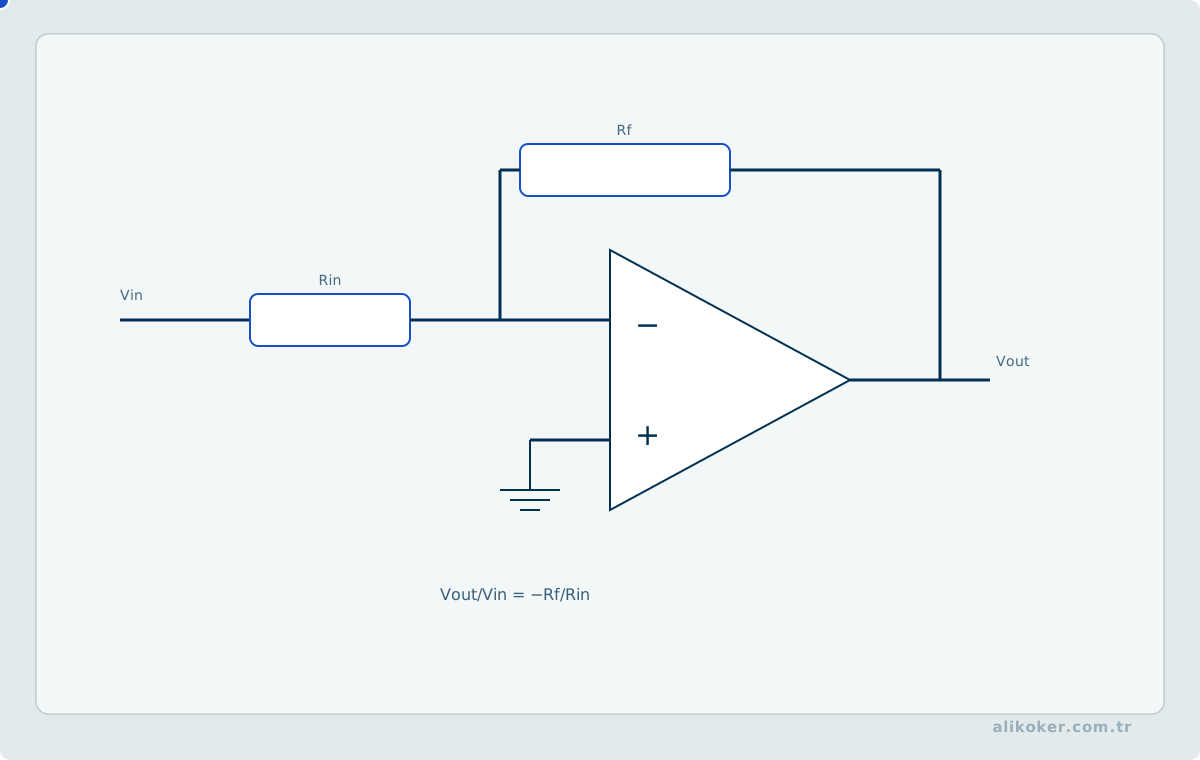
For the ideal negative-feedback model:
Vo / Vi = -Rf / RinThe inverting input is a virtual reference relative to the non-inverting input, not an actual short circuit.
Non-inverting amplifier
Vo / Vi = 1 + Rf/Rgfor the standard ideal topology.
Voltage follower
A follower ties output to the inverting input and drives the non-inverting input from the source. Ideal gain is one, with high input and low output impedance.
Summing and difference amplifiers
Multiple input resistors at the inverting node create a weighted summer. A difference amplifier subtracts scaled input voltages when resistor ratios are matched appropriately.
Differentiator and integrator
Ideal op-amp differentiator:
Vo = -RC dVi/dtIdeal integrator:
Vo = -(1/RC) integral Vi dtPractical circuits limit low/high-frequency gain to control noise, offsets and stability.
Unit 9: Analog and Digital Systems
An analog system represents information over a continuous range. A digital system represents information with discrete symbols/levels. Physical digital circuits are still analog electrical systems underneath; noise margins and timing allow continuous voltages to be interpreted reliably as discrete logic values.
Digital representation supports reproducible storage, logical processing, error detection and programmable behavior, but it introduces sampling, quantization, finite word length and interface requirements when interacting with analog signals.
ADC and DAC as the analog-digital boundary
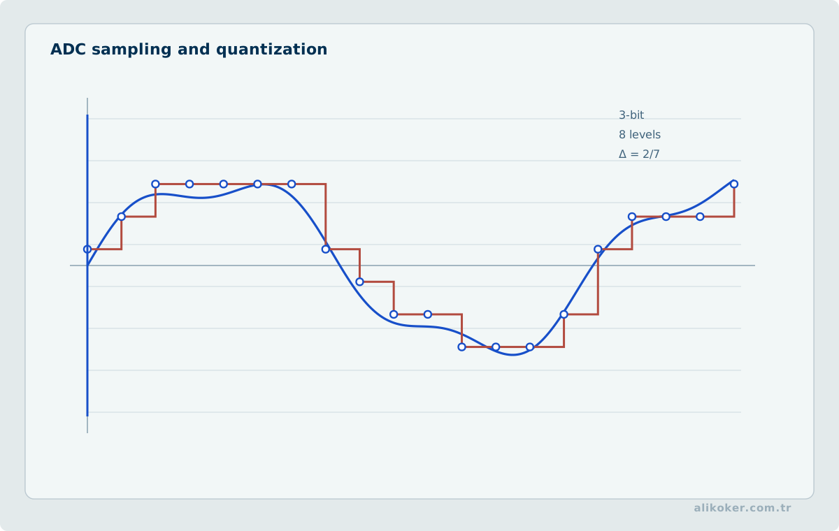
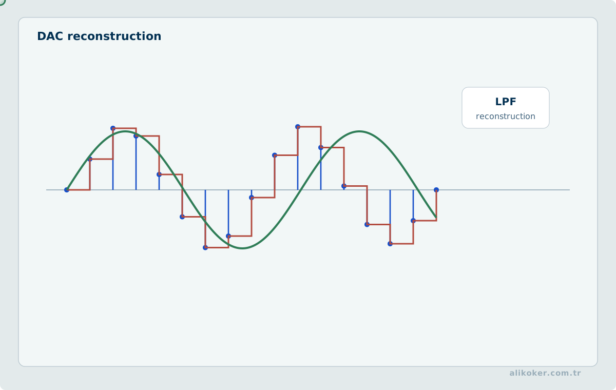
An analog-to-digital converter samples a continuous-time signal and maps amplitude to a finite code. Resolution alone does not define accuracy. Offset, gain error, differential/integral nonlinearity, aperture uncertainty, reference noise, and front-end noise also affect the result.
For an ideal N-bit converter with full-scale range V_FS, one LSB is approximately V_FS / 2^N.
Effective number of bits (ENOB) summarizes noise and distortion performance and is usually lower than the nominal resolution.
Sampling also requires an anti-aliasing decision. Frequencies above the usable Nyquist band can fold into the measured spectrum if the analog front end does not suppress them.
A DAC performs the reverse boundary transformation but still has finite settling time, monotonicity, glitch energy, reference error, and output-drive constraints.
Unit 10: Number Systems and Codes
Positional binary, octal and hexadecimal representations follow the same radix-weight principle discussed earlier. MSB denotes the most significant bit and LSB the least significant bit in a numerical word; physical transmission order is a separate interface convention.
Binary fractions use negative powers of two. BCD stores decimal digits independently. Weighted BCD codes assign explicit bit weights; Excess-3 is obtained by adding three to each decimal digit before four-bit encoding.
Gray code arranges consecutive codewords so only one bit changes. It is useful in position encoders and clock-domain pointer schemes because intermediate multi-bit transition ambiguity can be reduced, though correct synchronization still matters.
Parity adds simple redundancy. Octal/hexadecimal are compact notations rather than new machine encodings. Alphanumeric codes map characters to numeric values.
Unit 11: Boolean Algebra and Karnaugh Maps
Boolean variables take logical values. AND, OR and NOT form the basic operations; truth tables provide exhaustive finite behavior.
Identities, absorption and De Morgan's laws support simplification. SOP represents a function as a sum/OR of product terms; POS represents a product/AND of sum terms. Minterms correspond to truth-table 1 rows and maxterms to 0 rows in canonical forms.
Karnaugh maps use Gray adjacency to combine minterms/maxterms and eliminate variables. Don't-care states may join groups only when either output value is acceptable for those input combinations.
Unit 12: Logic Gates and Logic Families
AND, OR, NOT, NAND, NOR, XOR, XNOR and buffers are logical functions implemented by electronic circuits. Diode logic can implement limited functions but lacks inversion/gain. DTL and TTL are historically important bipolar logic families. CMOS became dominant for highly integrated digital systems because of its static-power and scaling characteristics, though dynamic switching power and leakage remain major design concerns.
Fan-in is the number of inputs a gate accepts; fan-out describes how many compatible inputs an output can drive under specified electrical constraints. Propagation delay is the time between a relevant input transition and the corresponding output transition.
Unit 13: Combinational Logic Circuits
Combinational design maps present inputs to present outputs. Analysis moves from circuit to expression/truth table; synthesis moves from behavior to simplified logic and then to gates.
NAND/NOR universal implementation follows Boolean transformation. Multiplexers route selected data and can synthesize functions. Encoders compress one-of-many signals; priority encoders resolve simultaneous requests. Decoders expand an input code to selected outputs and are used in address/control selection.
Unit 14: Arithmetic Logic Circuits
A one-bit comparator determines <, =, > for two bits; multi-bit comparison prioritizes the highest-order unequal bit.
Half/full adders implement binary addition. A ripple-carry adder cascades carries and therefore has width-dependent propagation delay.
A half subtractor handles two input bits; a full subtractor adds borrow-in. In practical arithmetic units, subtraction is commonly implemented by an adder using two's complement rather than by an entirely separate datapath.
Binary multiplication forms shifted partial products. Array multipliers arrange these products as a regular two-dimensional network; faster multipliers use recoding and reduction trees to shorten the carry-propagation path.
Unit 15: Sequential Circuits and Counters
A sequential circuit's outputs and next state depend on stored state as well as current inputs. An SR latch provides basic bistable storage; NAND and NOR versions use opposite active-level conventions.
A latch is level-sensitive; a flip-flop is commonly edge-triggered. A clock coordinates state transitions but does not eliminate setup, hold, propagation or clock-skew constraints.
An expanded state table lists current state, inputs, next state and outputs. Counter modulus is the number of states in its cycle. A decimal counter has modulus 10. A ring counter circulates a pattern through a register and trades extra storage for simple state decoding.
Sequential correctness requires both logical next-state equations and valid timing. A design that has the right state table can still fail physically if its clock period or setup/hold requirements are violated.
Overall Framework of Electronics I-II
The course sequence forms two connected layers:
charge, voltage, current
        ↓
R, L, C and circuit laws
        ↓
AC response and filters
        ↓
semiconductor physics
        ↓
diodes and transistors
        ↓
amplifiers and op-amps
        ↓
logic levels and Boolean algebra
        ↓
combinational/sequential digital circuits
Analog and digital electronics are not independent worlds. Logic gates are transistor circuits; timing and noise margins are analog properties; digital arithmetic is built from Boolean structures implemented in physical devices. The abstraction boundary is useful precisely because each lower layer supplies predictable behavior to the layer above it.
Tolerance, loading, and measurement uncertainty
Nominal schematic values are not exact physical values. Resistor tolerance, capacitor voltage and temperature dependence, amplifier offsets, ADC reference error, and supply variation should be considered together. A robust design works across credible worst cases, not only at the typical point.
Measurement equipment also becomes part of the circuit. Probe capacitance can disturb a fast node, while meter input resistance can load a high-impedance divider.
Tolerance analysis, Monte Carlo simulation, and corner testing are useful before production, but only to the extent that the model captures relevant parasitics. Differences between simulation and bench measurements are often evidence about missing physical effects.
Verifying circuit results by measurement
Circuit calculations use nominal values, while physical circuits include component tolerance, temperature, supply variation, and instrument loading. Simulation output, bench measurement, and datasheet limits are therefore different forms of evidence.
A measurement record should state probe type, bandwidth, grounding, sample rate, and supply conditions. Probe capacitance or instrument input resistance can materially change high-impedance or high-frequency nodes.
Design decisions should consider credible corner cases rather than one typical value. Datasheet min/typ/max limits, tolerance analysis, and bench measurements together define the conditions under which a circuit can be expected to operate.
From the Measurement Chain to Learning Systems
A learning model does not observe the physical world directly. It observes numerical samples produced by sensors and the analog front end. The strongest connection between electronics and AI therefore comes from the measurement chain that defines what the model can see, not from the generic statement that AI can be used in electronic systems.
A practical sensing path commonly follows this order:
physical quantity
↓
sensor / transducer
↓
amplification and analog filtering
↓
sampling and ADC
↓
digital signal
↓
feature or learned representation
↓
model
Information lost in the first half cannot always be recovered by choosing a larger model. Saturation clips information. Insufficient bandwidth suppresses fast changes. Poor grounding or electromagnetic interference raises the noise floor. An inadequate sampling rate creates aliasing. Limited ADC resolution can map distinct small variations to the same code. The model does not know the physical cause; it only learns the distribution presented to it.
In vibration, audio, or biosignal classification, for example, a field change in analog gain may become distribution shift if training data were acquired under a different gain. Sensor replacement, thermal drift, or supply noise can similarly alter the numerical distribution for the same physical event. Model accuracy and measurement accuracy can no longer be evaluated independently.
Signal-to-noise ratio is therefore not only an electronics metric. When useful signal energy disappears into noise, discriminative information is reduced. Analog filtering is also not made obsolete by downstream digital processing or machine learning; anti-alias filtering establishes the physical bandwidth before sampling.
The digital side creates another connection. Quantized models may perform inference with narrow integer arithmetic. Fixed-point representation, saturation, registers, counters, and data paths become direct constraints in resource-limited edge systems. The objective is not to imitate a general-purpose processor, but to realize the required dataflow with sufficient numerical quality and bounded energy.
The boundary must remain explicit. Electronics does not teach loss functions, generalization, or learning optimization. It teaches the physical reliability of the measurement that feeds those methods. A learning system inherits the limits of its sensor and acquisition chain; no statistical method can reconstruct information that was never captured.
Separating the Operating Point from Small-Signal Behaviour
Two different tasks are often mixed together in analog-electronics problems: finding the DC operating point and analysing small variations around that point. In a BJT or MOSFET amplifier, bias conditions come first. Whether the device is in cutoff, an active region, or saturation determines whether a later small-signal model is valid. A small-signal equivalent is not an alternative circuit that can replace the nonlinear device under every condition; it is a local linearization around an established operating point.
Operational-amplifier analysis has a similar boundary. The relation v+ ≈ v- is not a universal property that can be imposed on every op-amp circuit. It is a powerful consequence used when negative feedback is present, the output remains within the supply limits, and the device operates in its linear region. Once the output saturates or the feedback sign changes, carrying the same assumption forward produces an invalid solution.
For a diode, the piecewise-linear model, constant-voltage-drop model, and exponential model offer different balances between simplicity and accuracy. The appropriate model depends on the question. A first approximation of a rectifier may need only a constant drop, whereas temperature dependence, incremental resistance, or a precise current calculation requires a richer model.
The first question in an electronics solution is therefore often not “which formula should I use?” but “which operating region is the device in, and is my model valid there?” If the computed result violates the assumed region, the algebra may be correct while the circuit solution is not.
References
- Adel S. Sedra; Kenneth C. Smith. Microelectronic Circuits. Oxford University Press, 2010.
- James W. Nilsson; Susan A. Riedel. Electric Circuits. Pearson, 2011.
- M. Morris Mano; Michael D. Ciletti. Digital Design. Pearson, 2012.
- Pete Warden, D. S. TinyML: Machine Learning with TensorFlow Lite on Arduino and Ultra-Low-Power Microcontrollers. O’Reilly Media, 2019.
- Robert L. Boylestad; Louis Nashelsky. Electronic Devices and Circuit Theory. Pearson, 2012.