


Circuit Theory: Theory, Analysis, Design, and Practice


Comprehensive course notes covering circuit theory from fundamental electrical quantities and Kirchhoff’s laws to AC analysis, transient response, two-port networks, Fourier methods, and Laplace methods, combining theory, problem solving, and application.
Introduction — scope and approach. Circuit theory is the mathematical study of electrical quantities, ideal or approximate circuit elements, and the ways in which those elements are interconnected.
In the physical world, quantities such as:
sound
light
temperature
pressure
motion
magnetic field
chemical change
can be converted into electrical signals by suitable transducers.
A microphone converts sound pressure into voltage, a temperature sensor converts temperature into an electrical quantity, and a motor converts electrical energy into mechanical motion.
Circuit theory is therefore not merely about:
connecting resistors in series and parallel.
The broader chain is:
Physical phenomenon
↓
Electrical quantity
↓
Circuit model
↓
Equations
↓
Analysis
↓
Simulation
↓
Measurement
↓
Real circuit
Sound circuit analysis should be verified at four different levels:
1. Analytical solution
2. Numerical / programmed solution
3. Circuit simulation
4. Laboratory work with real components
The same engineering approach is preserved throughout the analysis.
The objective is not to memorize formulas, but:
to understand why a circuit behaves as it does, under which assumptions it can be modeled, and whether the calculated result is physically meaningful.
Unit 1: Fundamental Electrical Quantities and Circuit Elements
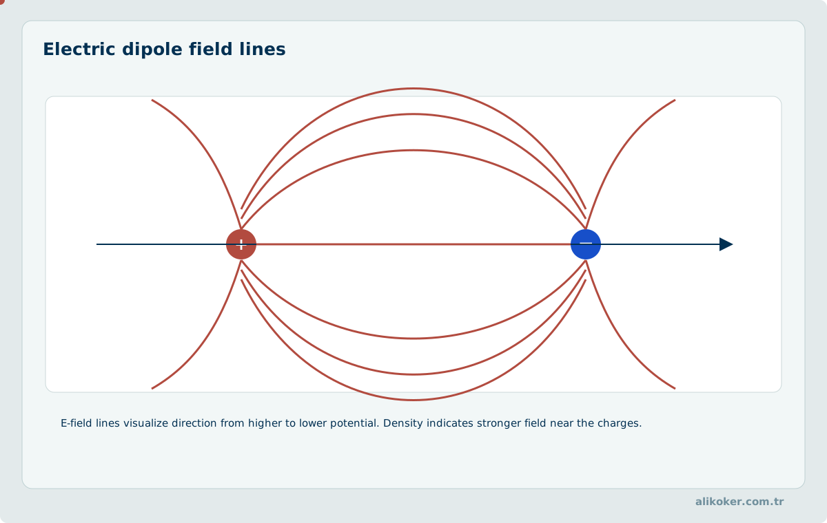
Seeing the electric field as flow lines makes direction, potential difference, and spatial strength easier to interpret than equations alone.
1.1. Scope of Circuit Theory
Circuit theory broadly addresses questions such as:
What is the voltage of a node?
How much current flows through a branch?
How much power does an element absorb or deliver?
How does the transient response develop after switching?
What are the phase relationships under AC excitation?
At which frequency does resonance occur?
How does a network appear externally as an equivalent circuit?
What is the frequency response of a circuit?
Which signal components does a filter pass?
These questions are fundamental in:
- power systems,
- communications,
- control,
- embedded systems,
- sensor interfaces,
- analog electronics,
- measurement systems.
1.2. Difference Between Circuit Theory and Electromagnetic Field Theory
Circuit theory treats a physical structure using a lumped-parameter model.
That is, effects such as:
R
L
C
are assumed to be concentrated in specific elements.
In reality:
- electric fields,
- magnetic fields,
- energy,
- charge
are distributed through space.
The circuit approximation works well only when the physical dimensions of the elements are sufficiently small relative to the wavelength of the signals involved and propagation delays can be neglected.
At high frequency:
conductor ≠ ideal wireand transmission-line or electromagnetic-field approaches may be required.
1.3. Lumped-parameter Assumption
One of the implicit fundamental assumptions of circuit theory is:
Voltage and current throughout each circuit element are assumed to propagate quickly enough to be described by a single time variable.
Thus, for an ideal wire:
same node → same potentialis assumed.
For a PCB trace operating at GHz frequencies or a cable extending for kilometers, however, this approximation may become inadequate.
1.4. Electric Charge
One of the fundamental electrical quantities is charge.
Symbol:
qUnit:
coulomb — CThe magnitude of the electron charge is approximately:
e ≈ 1.602 × 10^-19 Cand:
1 C ≈ 6.24 × 10^18corresponds approximately to that many elementary electron charges.
1.5. Electric Current
Current is the rate of change of charge with time:
        dq
i(t) = ----
        dt
Unit:
ampere — Aand:
1 A = 1 C/sThis definition matters.
Current is not:
“the amount of electrons,” but the net amount of charge passing through a cross-section per unit time.
1.6. Conventional Current Direction
In circuit theory, current direction is historically defined as:
the direction of positive-charge motionBecause the charge carriers in metals are usually electrons, their drift direction is opposite to conventional current direction.
This does not alter the circuit equations.
What matters is:
selecting a reference direction and using signs consistently.
1.7. Voltage
Voltage between two points is the difference in energy per unit charge:
        dw
v(t) = ----
        dq
Unit:
volt — Vwith:
1 V = 1 J/CVoltage is not an absolute quantity belonging to a single point; it is:
a potential difference between two points.
1.8. Reference Node
Node voltages are defined relative to a reference.
The node selected as:
0 Vmay be called:
- reference,
- common,
- ground.
The GND symbol in a schematic does not always mean a physical earth electrode.
Especially in:
- battery-powered devices,
- isolated power supplies,
- laboratory supplies,
“0 V” is often only the circuit's local reference.
1.9. Power
Instantaneous power in an element is:
p(t) = v(t)i(t)Unit:
watt — Wwith:
1 W = 1 J/sPower is:
the rate at which energy is transferred or converted.
1.10. Energy
Energy transferred over a time interval is:
         t2
w = ∫ p(t) dt
        t1
A resistor generally converts energy into heat.
A capacitor stores energy in its:
electric fieldand an inductor in its:
magnetic field1.11. Passive Sign Convention
If current enters the + voltage terminal of an element, then for:
p = vip > 0means that the element absorbs power, while:
p < 0means that it delivers power.
This is the passive sign convention.
It prevents one of the most common errors in power calculations.
1.12. Circuit Element Definition
In circuit analysis, physical components are represented by ideal mathematical elements.
Basic elements include:
resistor
capacitor
inductor
independent voltage source
independent current source
dependent source
switch
A real physical component may contain several of these effects simultaneously.
A real inductor, for example, may be modeled as:
ideal L
+
winding resistance
+
parasitic C
1.13. Ideal and Real Elements
An ideal model:
- simplifies analysis,
- reveals fundamental behavior,
- may be sufficient over a specified operating range.
A real component exhibits:
- tolerance,
- temperature dependence,
- parasitic elements,
- power limits,
- voltage limits,
- frequency dependence.
Therefore:
A model and a physical component are not the same thing.
1.14. Independent Voltage Source
An ideal voltage source forces its terminal voltage to:
v(t)=V_s(t)The connected circuit determines the current through it.
For an ideal source, theoretically:
i → ∞can be allowed.
A real source has:
- internal resistance,
- current limits,
- power limits.
1.15. Independent Current Source
An ideal current source forces:
i(t)=I_s(t)The connected circuit determines its terminal voltage.
A real current source has:
- compliance voltage,
- output resistance,
- power limits.
1.16. Dependent Sources
The value of a dependent source is controlled by another voltage or current in the circuit.
The four basic types are:
VCVS → voltage-controlled voltage source
VCCS → voltage-controlled current source
CCVS → current-controlled voltage source
CCCS → current-controlled current source
Dependent sources are very important in:
- transistor small-signal models,
- operational-amplifier models,
- active circuits.
1.17. Open Circuit
For an ideal open circuit:
i = 0but:
v ≠ 0may still hold.
An open circuit does not mean:
“nothing exists”; it means the current path is interrupted.
1.18. Short Circuit
For an ideal short circuit:
v = 0but:
i ≠ 0and the current may become very large depending on the source capability.
In real systems, short-circuit current is limited by:
- wire resistance,
- source internal resistance,
- fuses,
- current limiting.
1.19. Resistance
For an ideal linear resistor, Ohm's law is:
v = Riwhere:
R → resistancewith unit:
ohm — Ω1.20. Conductance
Conductance is defined by:
     1
G = ---
     R
Unit:
siemens — SOhm's law can also be written as:
i = GvUsing conductance can simplify algebra in parallel networks.
1.21. Power in a Resistor
Since:
P = VIand:
V = IRwe obtain:
P = I²Rand:
P = V²/RThese expressions calculate the same physical power from different known quantities.
1.22. Physical Limits of a Resistor
For a real resistor, knowing only:
R = 1 kΩis insufficient.
Also important are:
- tolerance,
- power rating,
- temperature coefficient,
- maximum working voltage,
- noise,
- package type.
For a:
1 kΩ, 0.25 Wresistor, sustained operation with:
P > 0.25 Wmay be inappropriate.
1.23. Temperature Coefficient
A real resistor may approximately vary as:
R(T)
≈
R(T0)[1 + α(T-T0)]
Thus:
Ris not absolutely constant under every condition.
Temperature coefficient can be critical in precision measurement circuits.
Unit 2: Resistive Networks, Kirchhoff Laws, and Circuit Analysis
Resistive-network analysis begins by fixing node and branch definitions and current reference directions. Choose nodal or mesh analysis according to the source configuration and form independent equations. Substitute the resulting currents and voltages into the original network, checking Kirchhoff's laws and power balance. If the result is physically inconsistent, revisit signs, the reference node, and dependent-source equations.
2.1. Series Connection
When there is no branching between two elements, the same current flows through them.
Series resistors add as:
R_eq =
R1 + R2 + ... + RN
The series equivalent is:
greater than each individual resistance.
2.2. Voltage Divider
If voltage V is applied across two series resistors:
R1
R2
then:
V_R2 =
V * R2/(R1+R2)
This is the voltage-divider relationship.
It assumes that no load is connected to the output.
2.3. Loading Effect
If a load:
R_Lis connected to the output of the divider, the lower branch becomes:
R2 || R_Land the new output is:
V_o =
V * (R2 || R_L)
/
[R1 + (R2 || R_L)]
Therefore:
Even the measuring instrument can affect the circuit.
2.4. Parallel Connection
Both terminals of parallel elements are connected to common nodes.
Their voltages are therefore equal.
For parallel resistors:
1/R_eq =
1/R1 + 1/R2 + ... + 1/RN
or:
G_eq =
G1 + G2 + ... + GN
2.5. Two Resistors in Parallel
For two resistors:
R_eq =
R1 R2 / (R1+R2)
The parallel equivalent is:
smaller than the smallest resistor in the parallel combination.
This is useful as a physical sanity check.
2.6. Current Divider
If total current I enters two parallel resistors:
I1 =
I * R2/(R1+R2)
and:
I2 =
I * R1/(R1+R2)
The conductance form is more intuitive:
I1 =
I * G1/(G1+G2)
Current divides in direct proportion to conductance.
2.7. Node
All points directly connected by ideal conductors with no ideal voltage drop between them form the same node.
A node is represented by:
one voltage valueCorrectly identifying nodes is the first requirement of nodal analysis.
2.8. Branch
A circuit element or group of elements between two nodes is called a branch.
A branch has a definable:
- current,
- terminal voltage.
2.9. Path, Loop, and Mesh
2.9.1. Path
A connection traversed through nodes and branches.
2.9.2. Loop
A closed path that returns to its starting node.
2.9.3. Mesh
A fundamental loop containing no other loop inside it.
The mesh concept is fundamental to mesh analysis in planar circuits.
2.10. Kirchhoff's Current Law — KCL
If charge accumulation at a node is negligible:
Σ i_k = 0Equivalently:
sum of currents entering
=
sum of currents leaving
KCL is the circuit-level expression of charge conservation.
2.11. Kirchhoff's Voltage Law — KVL
Around a closed loop:
Σ v_k = 0In other words:
voltage rises
=
voltage drops
KVL is related to conservation of energy and is a fundamental analysis tool under the lumped-circuit assumption.
2.12. Sign Discipline in Kirchhoff's Laws
Rather than memorizing signs in KCL and KVL, define reference directions.
For example, for KCL one may choose:
entering node → +
leaving node → -
Another convention is equally valid.
The critical requirement is:
not changing the sign convention within the same equation.
2.13. Conservation of Power
For ideal elements and sources in a circuit:
Σ p_k = 0must hold.
That is:
power delivered
=
power absorbed
This relationship is a strong verification tool for a solved circuit.
2.14. Conditions for Series-Parallel Reduction
If a circuit consists only of clearly identifiable series and parallel groups, equivalent-resistance reduction is sufficient.
In bridge circuits, however:
no pair of resistors
may be directly series or parallel
and methods such as:
- nodal analysis,
- mesh analysis,
- network transformations
may be required.
2.15. Star-delta Transformation
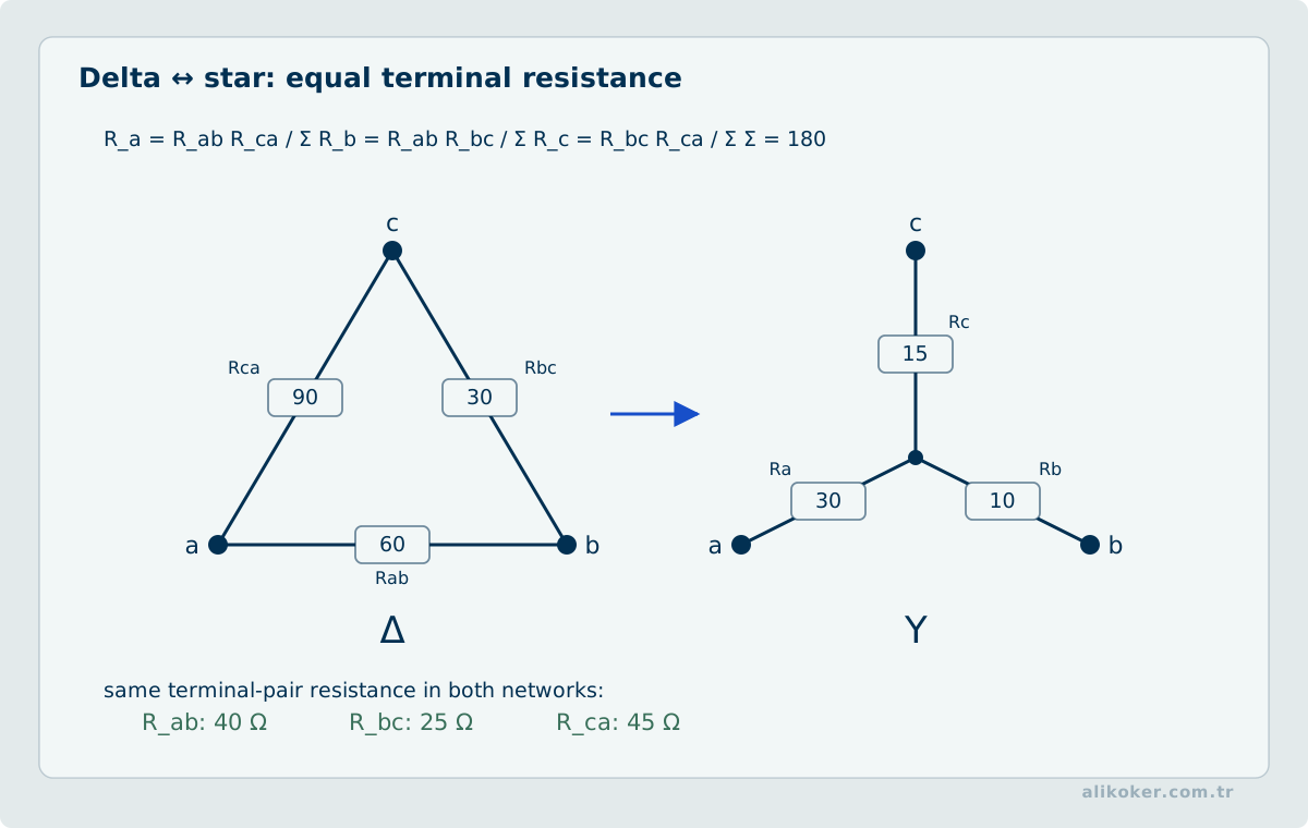
When a three-terminal resistive network cannot be reduced directly by series-parallel combinations, the:
Y ↔ Δtransformation may be used.
If the Δ resistances are:
R_ab
R_bc
R_ca
one star arm is obtained from a relationship such as:
R_a =
R_ab R_ca /
(R_ab+R_bc+R_ca)
This transformation is useful in:
- bridge networks,
- three-phase circuits.
2.16. Source Transformation
A voltage source:
V_sin series with:
R_scan be transformed into a current source:
I_s = V_s/R_sin parallel with the same R_s.
The two circuits have the same external terminal v-i behavior.
2.17. Limits of Source Transformation
Source transformation does not mean:
every internal voltage and current is identical.
Only the external terminal behavior is equivalent.
The same distinction applies to Thévenin and Norton equivalents.
2.18. Nodal-voltage Analysis
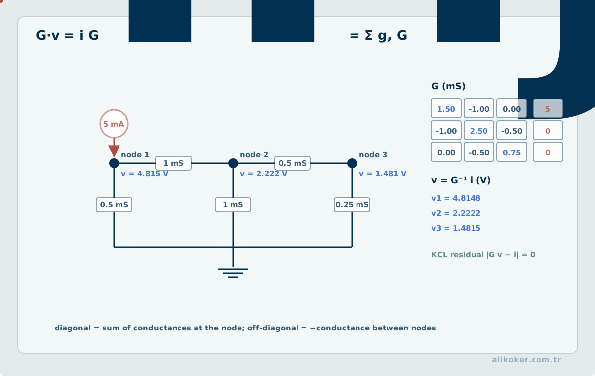
Nodal analysis solves unknown node voltages.
The basic sequence is:
1. Select the reference node
2. Define unknown node voltages
3. Write KCL at each required node
4. Express branch currents in terms of voltages
5. Solve the linear equation system
For resistive networks, the expression:
(V1-V2)/Ris used repeatedly.
2.19. Nodal-analysis Example
If a node:
Vis connected through:
R1 → V1
R2 → V2
R3 → 0
then:
(V-V1)/R1
+
(V-V2)/R2
+
V/R3
=
0
can be written.
This single equation determines the unknown V.
2.20. Supernode
If an ideal voltage source lies between two unknown nodes, the current through the source cannot be written directly with Ohm's law.
The two nodes are then treated together as a supernode.
Two equations are required:
1. KCL for the supernode
2. The voltage-source constraint equation
For example:
V1 - V2 = V_s2.21. Mesh-current Analysis
For a planar circuit, a current is assigned to each fundamental mesh.
The basic sequence is:
1. Identify the meshes
2. Select mesh-current directions
3. Write KVL for each mesh
4. Use current differences in shared elements
5. Solve the equation system
For a resistor shared by two meshes, for example:
i_R = I1 - I22.22. Supermesh
If an ideal current source lies between two meshes, its voltage is unknown.
Then write together:
- a supermesh KVL equation around the current source,
- the current-source constraint relating
I1-I2.
2.23. Comparison of Nodal and Mesh Analysis
A general selection heuristic is:
few nodes → nodal analysis
few meshes → mesh analysis
Nodal analysis is often shorter for current-source-heavy circuits, while mesh analysis can be shorter for planar circuits dominated by voltage sources.
Mathematically, both solve the same physical system.
2.24. Matrix Form
Nodal equations can be written as:
G v = iwhere:
G → conductance matrix
v → node-voltage vector
i → source vector
This structure is fundamental to computer-aided circuit analysis.
2.25. Modified Nodal Analysis — MNA
Classical nodal analysis alone is not sufficient for SPICE-like circuit solvers.
Additional unknowns are introduced for ideal voltage sources and certain other elements.
This method is known as:
Modified Nodal Analysis — MNAMNA solves:
- node voltages,
- selected source currents
within the same linear system.
2.26. Linear Circuit
If a circuit is linear, it satisfies:
T(a x1 + b x2)
=
a T(x1) + b T(x2)
This property underlies many methods, including:
- superposition,
- Thévenin,
- Norton,
- transfer functions.
2.27. Superposition Principle
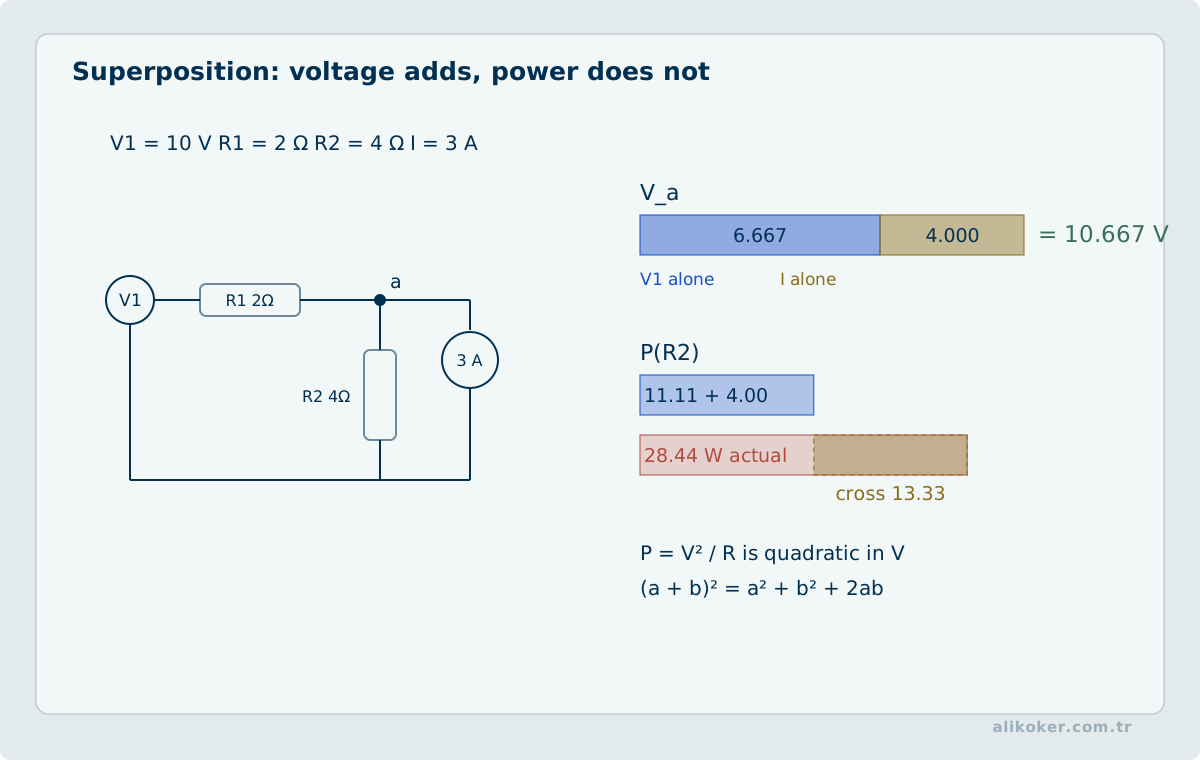
If a linear circuit contains multiple independent sources, the total response can be found as:
the algebraic sum of the responses
produced by each source acting alone
Other independent sources are deactivated:
ideal voltage source → short circuit
ideal current source → open circuit
Dependent sources remain active.
2.28. Superposition and Power
Superposition applies to:
voltage
current
Power is nonlinear because:
P = I²Ror:
P = V²/RTherefore:
In general, the total power cannot be found by simply adding the powers produced by the individual sources acting separately.
2.29. Thévenin's Theorem
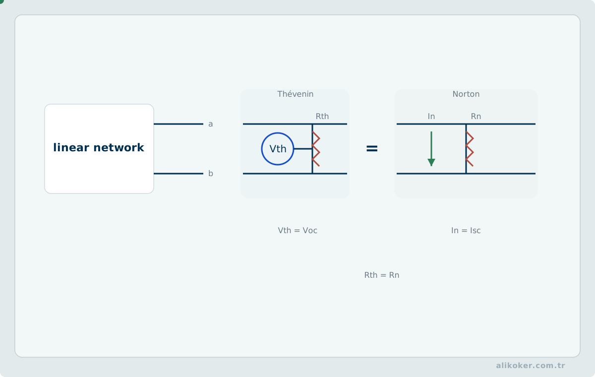
A linear two-terminal network can be represented externally by an ideal voltage source:
V_thin series with:
R_th[V_th] -- [R_th] -- loadwhere:
V_th = V_ocis the open-circuit voltage.
2.30. Thévenin Resistance
If only independent sources are present:
short independent voltage sources
open independent current sources
and calculate the resistance seen from the terminals.
Dependent sources must not be deactivated.
In that case, a test source can be used:
R_th = V_test/I_test2.31. Norton's Theorem
The same network can be represented by an ideal current source:
I_Nin parallel with:
R_Nwhere:
I_N = I_scand:
R_N = R_thThe Thévenin-Norton relationship is:
V_th = I_N R_th2.32. Meaning of an Equivalent Circuit
A Thévenin or Norton equivalent:
preserves the behavior seen from the selected two terminals, not the internal structure of the network.
As the load changes, the:
- load voltage,
- load current
match those of the original network.
Internal element currents need not be identical.
2.33. Maximum Power Transfer — DC
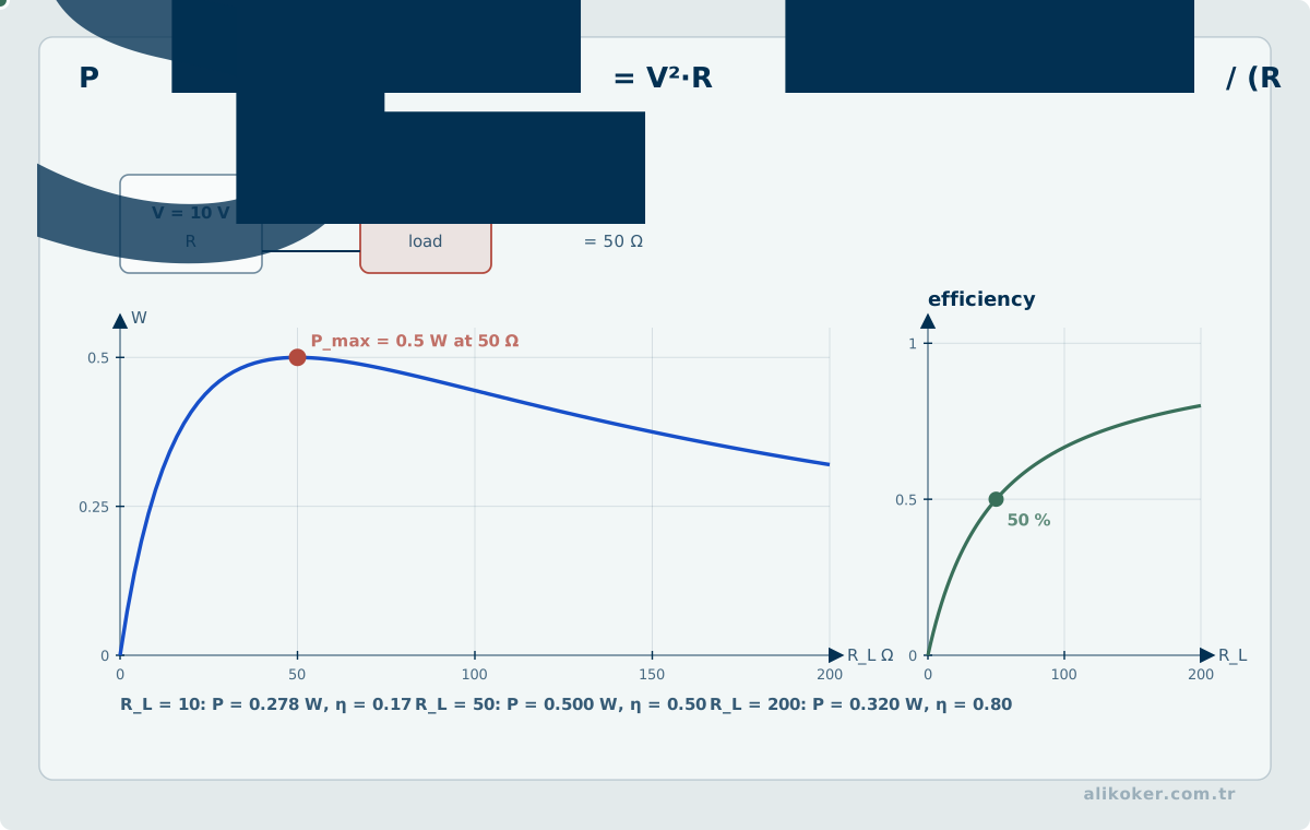
Let the Thévenin equivalent be:
V_th
R_th
with load:
R_LThe load power is:
P_L =
V_th² R_L /
(R_th + R_L)²
Maximum power is obtained when:
R_L = R_th2.34. Maximum Power Transfer Is Not Maximum Efficiency
When R_L = R_th, the source resistance dissipates as much power as the load.
For the ideal voltage-source plus series-resistance model, efficiency is:
η = 50%Therefore:
Maximum power transfer and maximum efficiency are not the same objective.
In power-transmission systems, low loss is often more important.
2.35. Millman's Theorem and Other Network Shortcuts
For networks containing several parallel voltage sources with series resistances, Millman's theorem can provide a direct expression for node voltage.
Such methods are not:
new physical laws replacing KCL or KVL.
They are shortcuts obtained by applying the fundamental laws to particular topologies.
2.36. Bridge Circuits
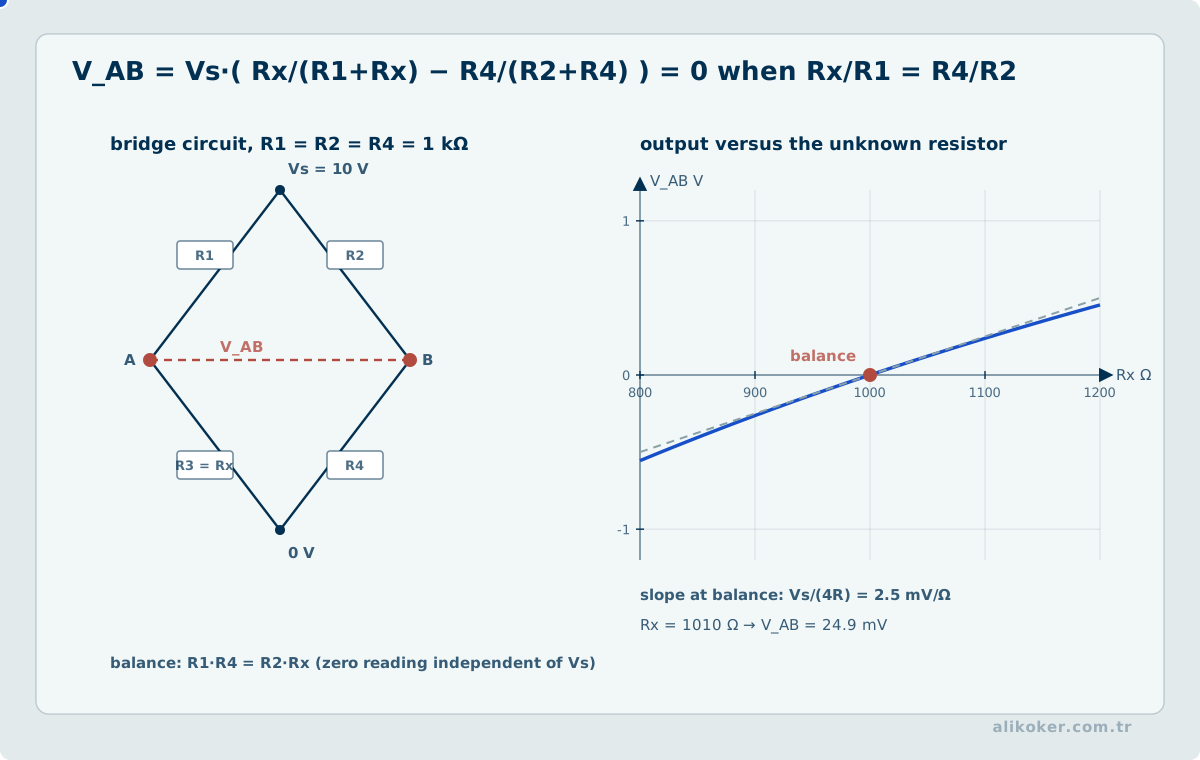
In a Wheatstone bridge, if:
R1/R2 = R3/R4then the current in the center branch can be zero.
This structure is important for:
- resistance measurement,
- strain gauges,
- precision sensor interfaces.
2.37. Modeling Extensions Beyond DC Resistive Analysis
In a circuit containing only resistors and constant sources, the algebraic relation:
v = Rimay be sufficient.
Once capacitors and inductors are introduced, the circuit includes:
derivatives
integrals
initial conditions
energy storage
It is no longer merely algebraic; it becomes:
a dynamic system.
2.38. Choosing the Solution Method from the Circuit Structure
The same circuit can often be solved by several methods; the important skill is choosing the representation that leaves the fewest unnecessary unknowns. Nodal analysis is economical when node voltages describe the network directly, while mesh analysis can be simpler for planar circuits with a small number of loops. Thévenin and Norton equivalents are useful when the question concerns what a particular load sees rather than every internal variable. Superposition separates the effects of independent sources in a linear circuit; it does not apply directly to derived nonlinear quantities such as power.
A numerical answer is not sufficient unless reference directions remain consistent. Current direction, voltage polarity, and the passive sign convention should be fixed before writing equations. If current enters the terminal defined as positive voltage, p = v i is positive when the element absorbs power. Reversing the reference changes the algebraic sign without changing the physical circuit. Many apparent Kirchhoff-law errors are therefore reference-definition errors.
Switching and transient problems require a separate check of the states immediately before and after the switching instant. The voltage of an ideal capacitor and the current of an ideal inductor cannot change discontinuously by a finite amount. These continuity conditions establish the initial state before a differential-equation or Laplace-domain solution is carried out. In the long-time DC limit, a capacitor approaches an open circuit and an inductor approaches a short circuit. Those limiting cases are inexpensive tests of whether a detailed solution is physically plausible.
A useful working order is therefore: identify topology and reference directions, select the simplest valid analysis method, solve the equations, then check units, power balance, and limiting cases. The point is not to memorize one preferred formula but to understand which model is valid under which conditions.
2.39. Reading Circuit Topology as a Graph
In circuit analysis, graph vertices represent electrical nodes and edges represent branches containing circuit elements. A reduced incidence matrix expresses Kirchhoff's current law as a linear system; branch admittances then yield nodal-voltage equations. The topology matrix is independent of component values, so a fixed connection pattern can be solved repeatedly for different parameters. This graph representation also helps detect disconnected nodes and redundant constraints.
- Relate node/branch topology to incidence and admittance matrices.
- Evaluate the electrical-equivalent effect of a broken connection separately from graph reachability.
- Show how structural single points of failure can be identified in a measurement network.
Unit 3: Capacitors, Inductors, and Transient Response
For a first-order transient, establish the pre-switch steady state to determine initial capacitor voltage or inductor current. Preserve the continuity constraint on the energy-storage state across switching. Derive the differential equation or equivalent time constant for the new configuration. Check the solution at the switching instant and in the long-time limit instead of trusting an exponential expression merely because it has the expected form.
3.1. Capacitor
The fundamental relation for an ideal capacitor is:
q = Cvwhich gives:
        dv
i = C ----
        dt
Unit:
farad — FA capacitor stores energy in an electric field.
3.2. Continuity of Capacitor Voltage
For an ideal capacitor:
v_C(t)cannot change by a finite amount in zero time.
Because:
i = C dv/dtan instantaneous voltage step would require infinite current.
Therefore, at a switching instant:
v_C(0+) = v_C(0-)This is one of the most important initial conditions in transient analysis.
3.3. Energy Stored in a Capacitor
W_C = 1/2 C v²An ideal capacitor does not dissipate energy.
It can:
- store energy,
- return energy to the source.
A real capacitor has:
- ESR,
- leakage resistance,
- dielectric losses.
3.4. Capacitor at DC Steady State
After a DC source has been applied long enough for steady state:
dv/dt = 0so:
i_C = 0and an ideal capacitor behaves as an:
open circuitThis statement applies only to DC steady state.
3.5. Capacitors in Parallel
Parallel capacitors have the same voltage.
Since total current is:
i =
(C1+C2+...+CN) dv/dt
we have:
C_eq =
C1 + C2 + ... + CN
3.6. Capacitors in Series
Series capacitors carry the same transferred charge.
Their equivalent capacitance is:
1/C_eq =
1/C1 + 1/C2 + ... + 1/CN
For two capacitors:
C_eq =
C1 C2/(C1+C2)
This resembles the inverse of the series-parallel rule for resistors.
3.7. Capacitive Voltage Division
For series capacitors:
V_k ∝ 1/C_kA smaller capacitance may therefore carry a larger voltage.
High-voltage series capacitor networks should not be designed from ideal algebraic division alone.
Real tolerances and leakage currents must be considered.
3.8. Real Capacitor
A real model may approximately include:
        ESR
---R----C---
    |
   leakage
and can be extended with parasitic inductance at high frequency.
Important parameters include:
- capacitance tolerance,
- ESR,
- ripple current,
- working voltage,
- temperature,
- dielectric type,
- aging.
3.9. Inductor
The fundamental relation for an ideal inductor is:
        di
v = L ----
        dt
Unit:
henry — HAn inductor stores energy in a magnetic field.
3.10. Continuity of Inductor Current
For an ideal inductor:
i_L(t)cannot change by a finite amount in zero time.
Because:
v = L di/dtan instantaneous current change would require infinite voltage.
At a switching instant:
i_L(0+) = i_L(0-)3.11. Energy Stored in an Inductor
W_L =
1/2 L i²
An ideal inductor does not dissipate energy.
A real coil, however, contains:
- winding resistance,
- core losses,
- parasitic capacitance.
3.12. Inductor at DC Steady State
Under long-term constant DC conditions:
di/dt = 0and:
v_L = 0so an ideal inductor behaves as a:
short circuitAgain, this is specifically a DC steady-state approximation.
3.13. Inductors in Series
If magnetic coupling is negligible:
L_eq =
L1 + L2 + ... + LN
If the coils influence one another magnetically, a mutual-inductance term:
Mmust be included.
This is addressed later.
3.14. Inductors in Parallel
Without coupling:
1/L_eq =
1/L1 + 1/L2 + ... + 1/LN
For two inductors:
L_eq =
L1 L2/(L1+L2)
3.15. First-order Circuit
A circuit with one independent energy-storage state is generally described by a first-order differential equation.
Classical examples are:
RC
RL
circuits.
The general response has the form:
x(t)
=
x(∞)
+
[x(0+) - x(∞)]e^(-t/τ)
3.16. Time Constant
In a first-order system:
τis the time constant.
For a simple RC circuit:
τ = RCand for an RL circuit:
τ = L/RIn a more general circuit, R is the Thévenin resistance seen from the terminals of the energy-storage element.
3.17. Physical Meaning of the Time Constant
For the natural response:
e^(-t/τ)the remaining difference is approximately:
t = τ   → 36.8%
t = 2τ  → 13.5%
t = 3τ  → 5%
t = 4τ  → 1.8%
t = 5τ  → 0.67%
Thus after roughly:
5τthe system is commonly considered practically settled.
3.18. RC Charging Circuit
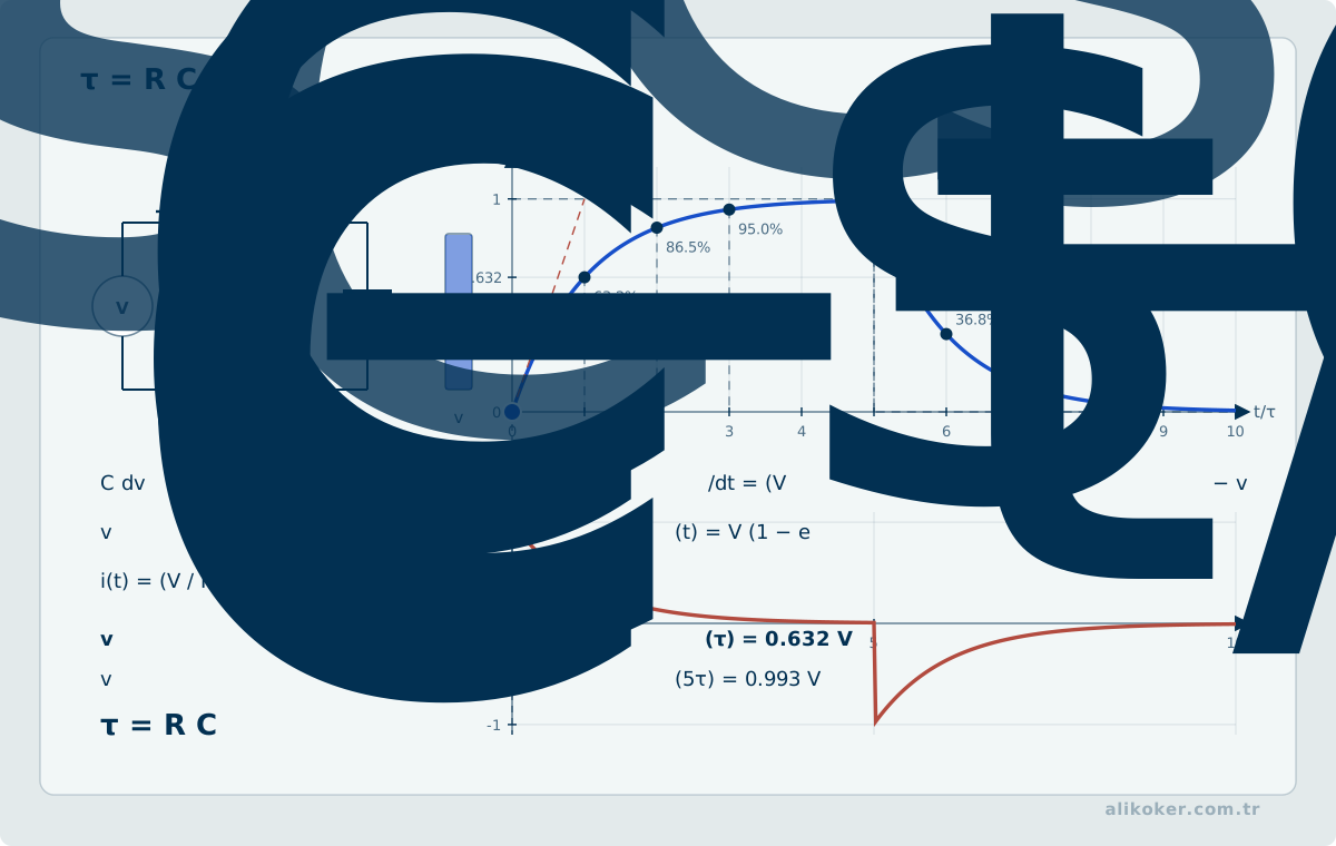
If a step voltage:
V_sis applied to a series R-C circuit with an initially uncharged capacitor:
v_C(t)
=
V_s(1-e^(-t/RC))
and:
i(t)
=
(V_s/R)e^(-t/RC)
Initially, the capacitor behaves approximately like a short circuit.
At long times it approaches open-circuit behavior.
3.19. RC Discharge
If a capacitor with initial voltage:
V_0discharges through a resistor:
v_C(t)
=
V_0 e^(-t/RC)
Depending on the chosen current reference direction:
i(t) =
-(V_0/R)e^(-t/RC)
may result.
3.20. RL Rising Response
If a DC step is applied to a series RL circuit:
i(t)
=
(V/R)(1-e^(-tR/L))
with time constant:
τ = L/RIf the initial inductor current is zero, it initially behaves like an open circuit.
At long times it approaches an ideal short circuit.
3.21. RL Natural Response
If an inductor with initial current:
I_0releases its energy through a resistor:
i(t)
=
I_0 e^(-tR/L)
The stored energy is converted into heat in the resistor.
3.22. Solution Sequence for Switching Problems
A good method for a first-order circuit is:
1. Solve the circuit for t<0
2. Find the initial stored energy
3. Apply the continuity condition
4. Solve the t→∞ circuit
5. Find τ
6. Write the general exponential response
For a capacitor:
v_C(0+)=v_C(0-)For an inductor:
i_L(0+)=i_L(0-)3.23. Natural and Forced Response
A circuit response can be separated as:
total response
=
natural response
+
forced response
The natural response is determined by:
- initial energy,
- system poles.
The forced response is produced by:
- external sources.
3.24. Zero-input and zero-state Response
Another decomposition is:
total response
=
zero-input response
+
zero-state response
3.24.1. Zero-input Response
External sources are zero while initial stored energy is present.
3.24.2. Zero-state Response
Initial energy is zero while external sources are present.
For linear systems, this separation follows from superposition.
3.25. Second-order Circuit
A circuit with two independent energy-storage states may be second order.
The classical example is an:
RLCcircuit.
The characteristic equation can generally be written as:
s² + 2αs + ω_0² = 03.26. Series RLC Circuit
For the natural response of a series RLC circuit:
α = R/(2L)and:
ω_0 = 1/√(LC)The roots are:
s1,2 =
-α ± √(α²-ω_0²)
3.27. Damping Cases
3.27.1. Overdamped
α > ω_0Two distinct real negative roots.
3.27.2. Critically Damped
α = ω_0A repeated real root.
3.27.3. Underdamped
α < ω_0Complex-conjugate poles.
The damped angular frequency is:
ω_d =
√(ω_0²-α²)
3.28. Underdamped Natural Response
The general form is:
x(t)
=
e^(-αt)
[
A cos(ω_d t)
+
B sin(ω_d t)
]
Two effects occur simultaneously:
oscillation → ω_d
envelope    → e^(-αt)
3.29. Critical Damping
In the critically damped case:
x(t)
=
(A+Bt)e^(-αt)
This is the boundary case that decays rapidly without oscillation.
3.30. Oscillation of RLC Energy
In an ideal LC circuit with:
R = 0energy moves continuously between:
capacitor electric field
↔
inductor magnetic field
Total energy remains constant in the ideal case.
Adding resistance reduces the energy on every cycle.
Checking time, power, and energy in an RC transient. An initially uncharged capacitor is charged from V_s = 10 V through R = 10 kΩ, with C = 100 µF. The time constant is τ = RC = 1 s, giving v_C(t) = 10(1 − e^(−t)) V. The voltage is approximately 6.32 V at t = 1 s and 9.93 V at t = 5 s. Initial current is i(0) = V_s/R = 1 mA and then decays exponentially. At steady state, stored energy is E_C = CV_s²/2 = 0.005 J. An ideal constant source delivers CV_s² = 0.010 J in total, so the other 0.005 J is dissipated by the series resistor. This energy balance independently checks the voltage solution against circuit physics. Real leakage and parasitic elements require additional modeling.
Unit 4: Sinusoidal Steady State, Phasors, and Resonance
4.1. Sinusoidal Signal
A general sinusoid can be written as:
x(t)
=
X_m cos(ωt+φ)
where:
X_m → peak amplitude
ω   → angular frequency
φ   → phase
4.2. Frequency and Period
ω = 2πfand:
T = 1/fwhere:
ω → rad/s
f → Hz
T → s
4.3. Phase
For two sinusoids at the same frequency:
x1 = A cos(ωt)
x2 = B cos(ωt+φ)
the phase difference is φ.
If:
φ > 0then x2 leads relative to the chosen cosine reference.
If:
φ < 0it lags.
4.4. RMS
The RMS value of a periodic signal is:
X_rms =
sqrt[
(1/T) ∫_0^T x²(t) dt
]
For a sinusoid:
X_rms =
X_m/√2
RMS can be interpreted as:
the equivalent DC value that produces the same average heating power in the same resistor.
4.5. Average Value
The average of a pure sinusoid over one full period is:
0while:
RMS ≠ 0This distinction is fundamental in AC power analysis.
4.6. Role of Complex Numbers in Circuit Theory
A complex number has the form:
z = a + jbPolar representation is:
z =
|z| ∠θ
or:
z =
|z|e^(jθ)
Euler's relation:
e^(jθ)
=
cosθ + j sinθ
turns phase analysis into algebra.
4.7. Phasor
Under sinusoidal steady-state conditions, the signal:
v(t)
=
V_m cos(ωt+φ)
can be represented by the phasor:
V = V_rms ∠φBecause the time-dependent factor:
cos(ωt)is common, complex algebra can replace differential equations.
4.8. Limits of the Phasor Method
The phasor method is appropriate for:
- LTI circuits,
- a single frequency,
- sinusoidal steady state.
It does not directly represent transients.
Different frequencies are not mixed in a single phasor equation.
For a multifrequency signal, each frequency can be analyzed separately and the results superposed.
4.9. Resistor Impedance
For a resistor:
V = RIso:
Z_R = RVoltage and current are in phase.
4.10. Inductive Impedance
From:
v = L di/dtin the phasor domain:
V = jωL ITherefore:
Z_L = jωLFor an inductor, voltage leads current by:
+90°4.11. Capacitive Impedance
From:
i = C dv/dtin the phasor domain:
I = jωC VTherefore:
Z_C =
1/(jωC)
=
-j/(ωC)
In a capacitor, current leads voltage by:
+90°4.12. Reactance
Impedance can be written as:
Z = R + jXwhere:
R → resistance
X → reactance
For an inductor:
X_L = +ωLFor a capacitor:
X_C = -1/(ωC)4.13. Impedance Magnitude and Phase
If:
Z = R+jXthen:
|Z| = √(R²+X²)and:
θ = atan2(X,R)AC Ohm's law is:
V = ZI4.14. Admittance
Admittance is defined as:
Y = 1/Zand may be written:
Y = G + jBwhere:
G → conductance
B → susceptance
Admittance is often more convenient for parallel AC circuits.
4.15. Inductive and Capacitive Susceptance
For an ideal capacitor:
Y_C = jωCFor an ideal inductor:
Y_L =
1/(jωL)
=
-j/(ωL)
Thus capacitive susceptance is positive and inductive susceptance is negative under this convention.
4.16. Series Connection in AC Circuits
Series impedances add:
Z_eq =
Z1+Z2+...+ZN
The current is:
I = V/Z_eqand each element voltage is:
V_k = I Z_k4.17. Parallel Connection in AC Circuits
In parallel networks it is often easier to use:
Y_eq =
Y1+Y2+...+YN
The total current is:
I = VY_eq4.18. AC Nodal and Mesh Analysis
The methods used for DC circuits:
- KCL,
- KVL,
- nodal analysis,
- mesh analysis,
- Thévenin,
- Norton
remain valid under sinusoidal steady-state conditions.
The main difference is using:
Zinstead of:
Ror:
Yinstead of:
GThis demonstrates the strong internal consistency of circuit theory.
4.19. Frequency-dependent Voltage Divider
In an AC circuit:
V_o =
V_i Z_2/(Z_1+Z_2)
the divider is frequency dependent.
This single equation underlies the behavior of:
- RC low-pass filters,
- RC high-pass filters,
- RLC resonance,
- passive filters.
4.20. RC low-pass Filter
For a series R-C circuit with output across the capacitor:
         1
H(jω)=---------
       1+jωRC
The cutoff frequency is:
ω_c = 1/RCor:
f_c =
1/(2πRC)
4.21. RC high-pass Filter
If the output is taken across the resistor:
        jωRC
H(jω)=---------
       1+jωRC
Low frequencies are attenuated while higher frequencies are passed more strongly.
4.22. Cutoff Frequency
At the cutoff frequency of a first-order RC filter:
|H| =
1/√2
In decibels:
20log10(1/√2)
≈ -3.01 dB
The cutoff frequency is therefore often called the:
-3 dB point4.23. Bode Magnitude Slope
A first-order pole contributes approximately:
-20 dB/decadeafter its break frequency.
A first-order zero contributes:
+20 dB/decadeThis approximation enables rapid interpretation of higher-order filter behavior.
4.24. Series Resonance
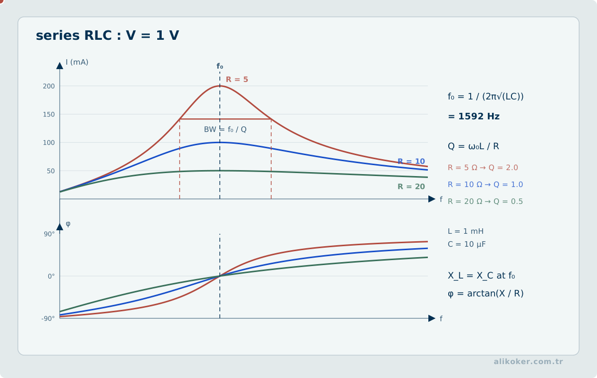
The impedance of a series RLC circuit is:
Z =
R + j(ωL - 1/(ωC))
At resonance:
ωL =
1/(ωC)
Therefore:
ω_0 =
1/√(LC)
and:
f_0 =
1/(2π√(LC))
4.25. Behavior at Series Resonance
At resonance:
Z = RFor an ideal series RLC circuit, impedance is minimum.
Thus, for fixed source voltage, current is maximum.
Moreover:
V_Land:
V_Cmay be large and opposite in phase.
Individual element voltages can exceed the source voltage.
4.26. Quality Factor — Q
For a series RLC circuit:
Q =
ω_0 L/R
and equivalently:
Q =
1/(ω_0 C R)
A high Q implies:
- sharp resonance,
- narrow bandwidth,
- larger oscillation of reactive energy.
4.27. Bandwidth
For an ideal classical series RLC circuit:
BW =
ω_2 - ω_1
=
R/L
and:
Q =
ω_0/BW
In hertz:
Q =
f_0/(f_2-f_1)
4.28. Parallel Resonance
For a parallel RLC circuit, resonance is examined through:
Im{Y}=0For an ideal parallel LC circuit, the resonant frequency is again:
ω_0 = 1/√(LC)At this point, input admittance approaches a minimum and impedance a maximum.
4.29. Benefits and Risks of Resonance
Resonance is useful in:
- radio tuning,
- filters,
- oscillators,
- impedance matching.
When unwanted, it can cause:
- excessive voltage,
- excessive current,
- vibration,
- component stress.
Resonance is therefore:
a physical property that is either exploited or suppressed.
4.30. Three Levels of AC Analysis
It is useful to think of sinusoidal circuit analysis at three levels:
1. Time domain:
v(t), i(t)

2. Phasor domain:
V, I, Z

3. Power domain:
P, Q, S, power factor
The same physical circuit is represented differently according to the question being asked.
Unit 5: AC Power, Magnetic Coupling, Transformers, and Three-Phase Systems
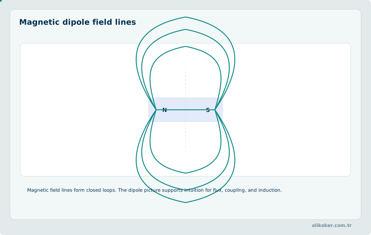
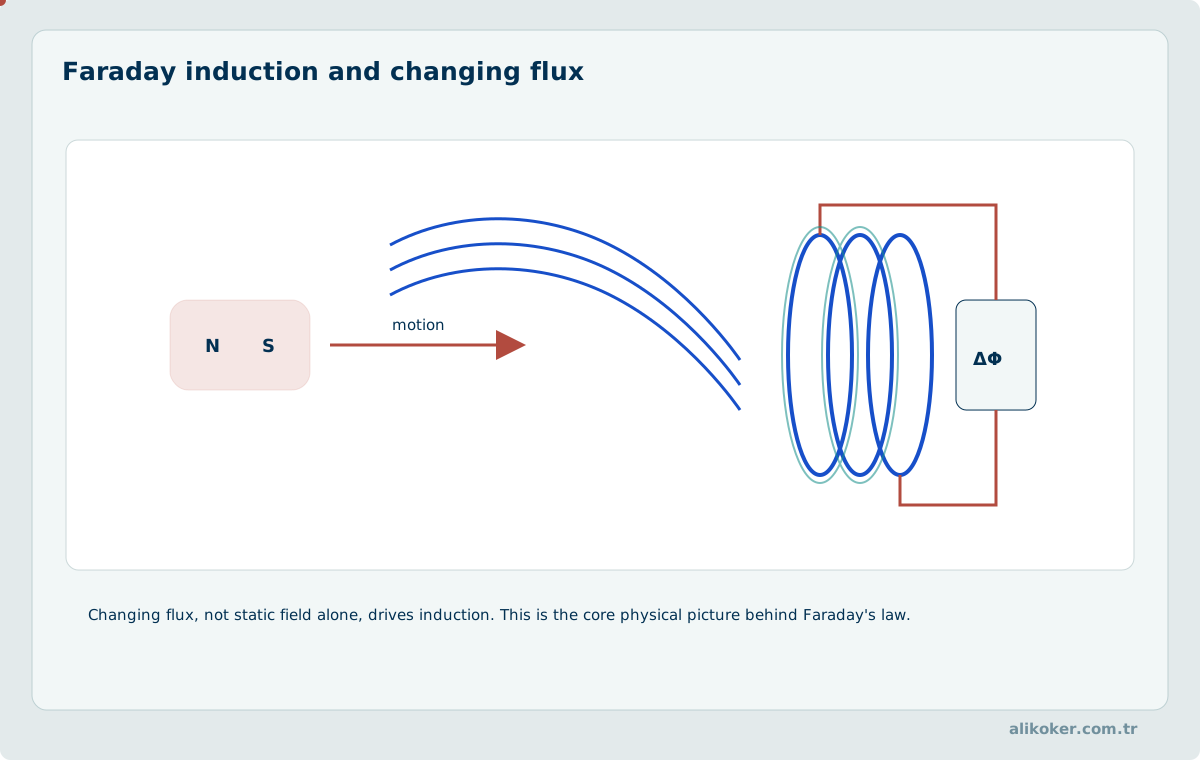
Magnetic coupling and transformer behavior become more intuitive when dipole loops and changing flux are visualized together.
5.1. Instantaneous Power — AC
Let:
v(t)=V_m cos(ωt+θ_v)and:
i(t)=I_m cos(ωt+θ_i)Instantaneous power is:
p(t)=v(t)i(t)Using trigonometric identities:
p(t)
=
V_rms I_rms cosφ
+
V_rms I_rms cos(2ωt+θ_v+θ_i)
so power contains a constant component and a component at twice the frequency.
Here:
φ = θ_v - θ_i5.2. Average Real Power
The average over one period is:
P =
V_rms I_rms cosφ
Unit:
watt — WThis power corresponds to net energy conversion into forms such as:
- heat,
- light,
- mechanical work,
- chemical change.
5.3. Reactive Power
Reactive power is defined as:
Q =
V_rms I_rms sinφ
Unit:
varUnder the common sign convention:
inductive load → Q > 0
capacitive load → Q < 0
5.4. Apparent Power
The magnitude of apparent power is:
|S| =
V_rms I_rms
Unit:
VAComplex power is defined as:
S = P + jQ5.5. Complex Power
When phasors use RMS values:
S = V I*where:
I*is the complex conjugate of the current phasor.
Omitting the conjugate produces an incorrect sign for reactive power.
5.6. Power Triangle
        Q
        |
        |
        |
        |  \ S
        |φ
        +---->
          P
with:
|S|² = P² + Q²5.7. Power Factor
pf =
P/|S|
=
cosφ
Power factor indicates:
how much of the RMS current drawn by a load contributes to real power transfer.
A low power factor can require higher current for the same real power.
5.8. Leading and Lagging Power Factor
For an inductive load, current lags voltage:
lagging pfFor a capacitive load, current leads voltage:
leading pfThis description carries more information than the numerical value of cosφ alone.
5.9. Power-factor Correction
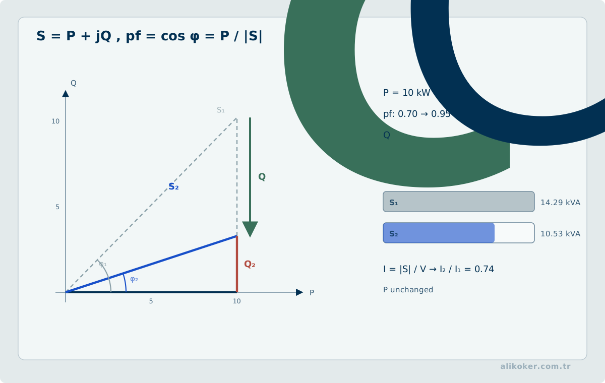
The positive reactive power of an inductive load:
Q_Lcan be reduced by adding capacitance.
The required capacitive reactive power can be calculated, under the chosen sign convention, using:
Q_C =
P(tanφ_2 - tanφ_1)
For a single-phase shunt capacitor:
|Q_C| =
ω C V_rms²
so:
C =
|Q_C|/(ωV_rms²)
5.10. Purpose of power-factor Correction
The usual objective is:
same real power
+
lower line current
This can reduce:
- transmission losses,
- cable voltage drop,
- transformer and generator loading.
Excessive compensation, however, can make the system capacitive or create resonance problems.
5.11. AC Power in a Pure Resistor
For a resistor:
φ = 0and:
Q = 0Thus:
P = V_rms I_rms5.12. Average Power in a Pure Inductor
For an ideal inductor:
φ = +90°so:
P = 0while:
Q > 0Energy moves back and forth each period between the source and the magnetic field.
5.13. Average Power in a Pure Capacitor
For an ideal capacitor:
φ = -90°and:
P = 0Reactive power satisfies:
Q < 0Energy is exchanged between the source and the electric field.
5.14. Maximum Average Power Transfer — AC
If the source Thévenin impedance is:
Z_th =
R_th + jX_th
maximum average load power is obtained when:
Z_L =
Z_th*
that is:
R_L = R_th
X_L = -X_th
This is called conjugate impedance matching.
5.15. Impedance Matching
Impedance matching is not used only for maximum power transfer.
In communications and high-frequency systems it is also used for:
- reducing reflections,
- establishing specified source-load conditions,
- managing transfer efficiency.
In low-frequency power systems, maximum power transfer is usually not the primary objective.
5.16. Magnetic Coupling
If the magnetic fields of two coils interact, a change in current in one coil induces voltage in the other.
This effect is modeled by mutual inductance:
MFor example:
v1 =
L1 di1/dt
± M di2/dt
and:
v2 =
L2 di2/dt
± M di1/dt
5.17. Mutual Inductance
The ideal coupling bound is:
|M| ≤ √(L1 L2)The coupling coefficient is:
k =
M/√(L1L2)
with:
0 ≤ k ≤ 1and:
k = 1represents ideal complete coupling.
5.18. Dot Convention
The sign of the mutual-inductance term depends on coil orientation.
Circuit diagrams use the dot convention.
A useful intuition is:
- if both reference currents enter dotted terminals, the mutual terms have the same sign,
- if one current enters a dotted terminal while the other leaves, the sign is opposite.
The sign must be written carefully according to the actual schematic.
5.19. Energy in Coupled Coils
For two coupled coils, energy can take the form:
W =
1/2 L1 i1²
+
1/2 L2 i2²
±
M i1 i2
The sign of the mutual term depends on the reference directions.
For a passive physical system, the energy function must satisfy appropriate positivity conditions.
5.20. Ideal Transformer
Let the turns ratio be:
n =
N1/N2
The voltage relationship is:
V1/V2 =
N1/N2 =
n
Current magnitudes are inversely proportional:
I1/I2 =
N2/N1 =
1/n
with appropriate sign directions.
5.21. Power in an Ideal Transformer
In the ideal case there are no losses:
P_in = P_outand the magnitude relationship:
V1 I1 =
V2 I2
holds.
A real transformer has:
- copper loss,
- core loss,
- leakage flux,
- magnetizing current.
5.22. Reflected Impedance
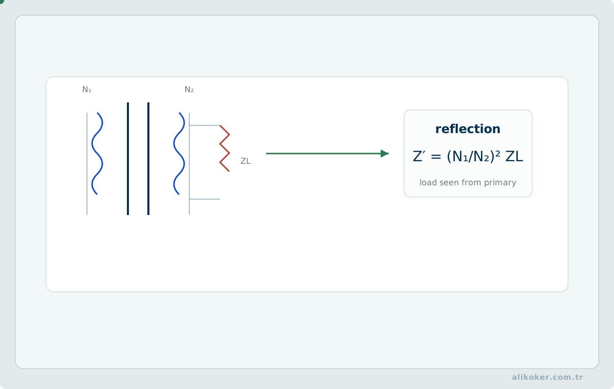
A load impedance on the secondary:
Z_Lis seen from the primary as:
Z_in =
n² Z_L
This property is important for impedance matching.
5.23. Real Transformer Equivalent Circuit
A more realistic model includes:
R1, R2 → winding resistances
X_l1, X_l2 → leakage reactances
R_c → core loss
X_m → magnetizing reactance
The ideal transformer is the central energy-transfer element of this model.
5.24. Three-phase System
In an ideal balanced three-phase system, three sinusoidal voltages have the same frequency and are separated by:
120°For example:
v_a =
V_m cos(ωt)

v_b =
V_m cos(ωt-120°)

v_c =
V_m cos(ωt+120°)
5.25. Rationale for Three-Phase Systems
Three-phase systems provide:
- a natural rotating field in electric machines,
- smoother power transfer,
- efficient use of conductor material,
- suitability for high-power systems.
They are therefore standard in power generation, transmission, and motor systems.
5.26. Balanced Three Phase
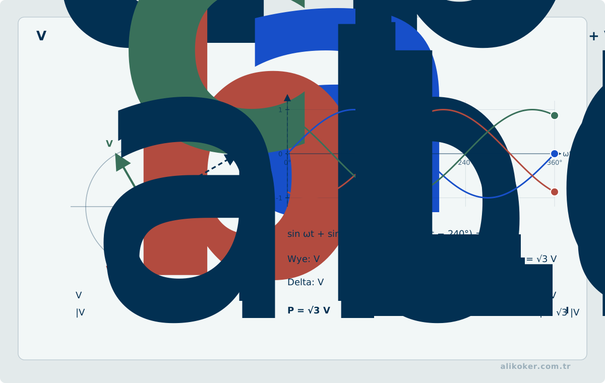
In a balanced system:
|V_a|=|V_b|=|V_c|and the phases are separated by:
120°For a balanced wye-connected load:
I_a + I_b + I_c = 0so neutral current is zero.
5.27. Wye Connection — Y
In a wye-connected load, one terminal of each phase is connected to a common neutral point.
If phase voltage is:
V_phand line voltage is:
V_Lthen for a balanced positive-sequence system:
|V_L| =
√3 |V_ph|
and:
I_L = I_ph5.28. Delta Connection — Δ
In a delta-connected load, phase elements are connected between line conductors.
Then:
V_L = V_phand, under balanced conditions:
|I_L| =
√3 |I_ph|
with the phase relationships also taken into account.
5.29. Total Real Power in Three Phase
For a balanced load:
P_total =
3 V_ph I_ph cosφ
or equivalently:
P_total =
√3 V_L I_L cosφ
Reactive power:
Q_total =
√3 V_L I_L sinφ
Apparent power:
|S_total| =
√3 V_L I_L
5.30. Instantaneous Total Power in Three Phase
An important property of a balanced three-phase system is:
Although instantaneous power in each individual phase oscillates, the total instantaneous power is constant under ideal balanced conditions.
This is one of the main reasons three-phase motors can produce smoother torque.
5.31. Phase Sequence
The order in which the phase waveforms reach their peaks may be:
abcor:
acbPhase sequence can determine motor rotation direction.
Swapping two line phases reverses the sequence.
5.32. Unbalanced Three Phase
If the loads differ:
Z_a ≠ Z_b ≠ Z_cthen the system is unbalanced.
With a neutral conductor, the phases can be solved separately using nodal analysis.
Without a neutral, the star-point voltage may shift.
An unbalanced system should not be treated blindly with a single-phase equivalent.
5.33. Symmetrical Components
In advanced power-system analysis, unbalanced three-phase systems can be decomposed into:
positive sequence
negative sequence
zero sequence
components.
This is a power-system method beyond introductory circuit theory, but it is a natural extension of phasor and linear-transformation concepts.
Unit 6: Two-Port Networks, Network Functions, Laplace, and Fourier
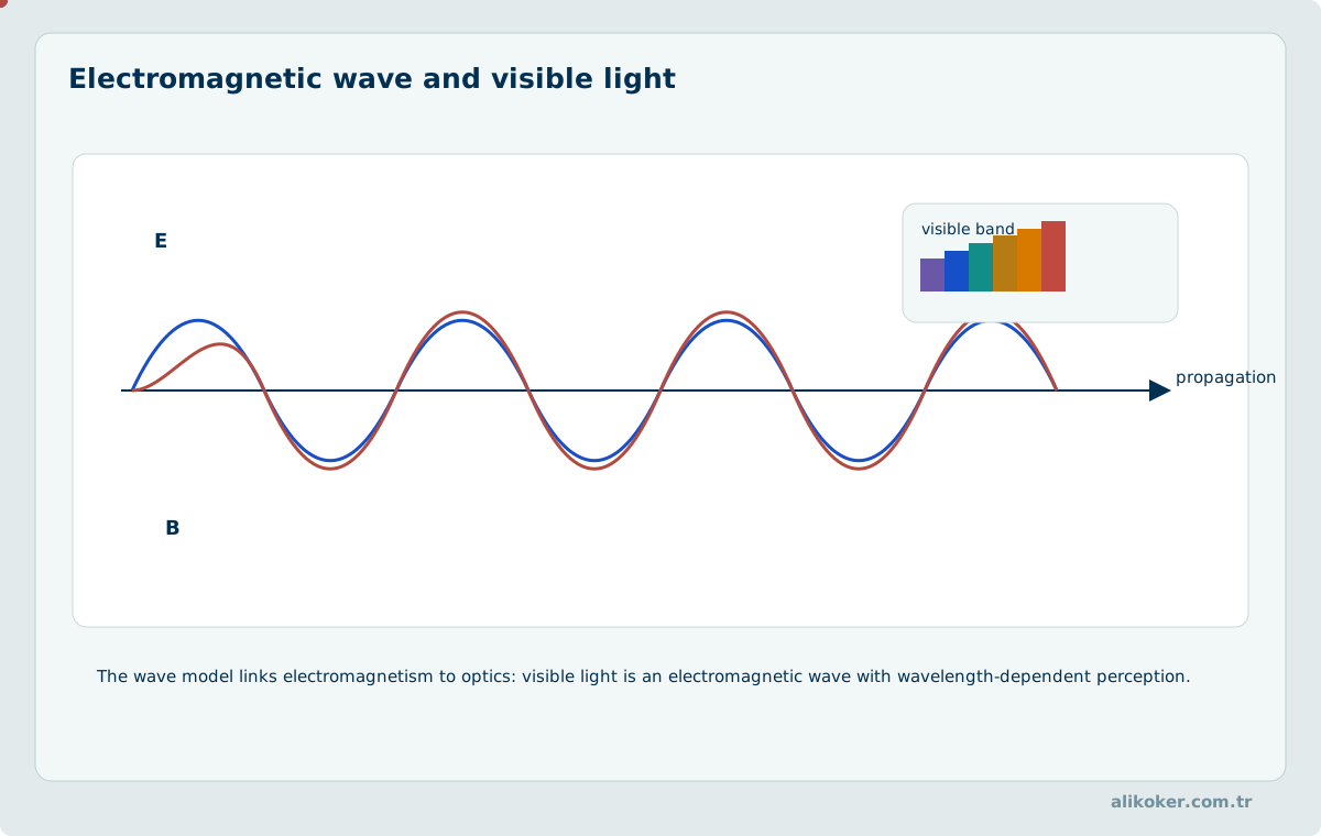
From Maxwell's perspective, circuit models are engineering-scale simplifications of electromagnetic field behavior under stated assumptions.
6.1. Two-port Network
A circuit block can be studied as:
Port 1 ↔ network ↔ Port 2with four terminals.
At each port:
V1, I1
V2, I2
are defined.
The objective is to hide internal detail and express external input-output behavior through parameters.
6.2. Significance of Two-Port Network Models
Structures such as:
- amplifiers,
- filters,
- transmission-line sections,
- cascaded circuits,
- transistor small-signal models
can be represented as two-port networks.
This simplifies modular circuit analysis.
6.3. z-parameters
Impedance parameters are:
V1 =
z11 I1 + z12 I2

V2 =
z21 I1 + z22 I2
or:
[V1]   [z11 z12][I1]
[V2] = [z21 z22][I2]
The parameters can be determined from open-circuit conditions.
6.4. y-parameters
Admittance parameters are:
I1 =
y11 V1 + y12 V2

I2 =
y21 V1 + y22 V2
Short-circuit conditions can make these natural for measurement and calculation.
6.5. h-parameters
Hybrid parameters are:
V1 =
h11 I1 + h12 V2

I2 =
h21 I1 + h22 V2
They have historically been widely used for transistor small-signal models.
6.6. ABCD Parameters
Transmission parameters can be written, depending on the current sign convention, as:
[V1]   [A B][ V2]
[I1] = [C D][-I2]
They are especially useful for cascaded networks.
If two networks are connected in cascade:
T_total =
T1 T2
is obtained by matrix multiplication.
6.7. Reciprocity
For some passive linear bilateral networks, reciprocity conditions such as:
z12 = z21may hold.
For ABCD parameters, under an appropriate definition:
AD-BC=1is one reciprocity condition.
An active network is not necessarily reciprocal.
6.8. Symmetry
A two-port network may be symmetric if it behaves identically from its input and output sides.
For z-parameters, a condition such as:
z11 = z22may result.
Symmetry and reciprocity are not the same concept.
6.9. Network Function
For an LTI circuit under zero initial conditions, a network function can be defined as:
H(s) =
Output(s)/Input(s)
For example:
V_o(s)/V_i(s)is a voltage transfer function.
6.10. Poles and Zeros
If:
H(s)=N(s)/D(s)then:
N(s)=0 → zeros
D(s)=0 → poles
Poles determine:
- natural response,
- stability,
- time constants.
Zeros can create:
- frequency attenuation,
- transient-response shaping,
- transmission zeros.
6.11. Circuit Poles and Natural Response
For the RC circuit:
H(s)=1/(1+sRC)the pole is:
s=-1/RCThe time-domain natural response:
e^(-t/RC)follows directly from this pole.
This demonstrates the relationship:
s-plane
↔
time domain
6.12. Laplace Transform
The unilateral Laplace transform is:
X(s) =
∫_0^∞ x(t)e^(-st)dt
The general bilateral definition is:
X(s) =
∫_-∞^∞ x(t)e^(-st)dt
For circuit transients, the unilateral transform is commonly used because it naturally incorporates initial conditions.
6.13. Analytical Power of the Laplace Transform
A time-domain problem containing:
derivatives
integrals
differential equations
becomes an:
algebraic equationin the Laplace domain.
For example:
L{dx/dt}
=
sX(s)-x(0-)
so the initial condition enters the equation directly.
6.14. Resistor in the s-domain
For a resistor:
V(s)=R I(s)therefore:
Z_R(s)=R6.15. Inductor in the s-domain
For an inductor:
v=L di/dtwe obtain:
V(s)
=
LsI(s)
-
L i(0-)
With zero initial conditions:
Z_L(s)=LsThe initial current can also be represented by an equivalent source.
6.16. Capacitor in the s-domain
For:
i=C dv/dtwe obtain:
I(s)
=
CsV(s)
-
C v(0-)
With zero initial conditions:
Z_C(s)=1/(Cs)The initial voltage can be included as an equivalent source.
6.17. Circuit Methods in the Laplace Domain
In the s-domain, the following methods remain applicable:
- KCL,
- KVL,
- nodal analysis,
- mesh analysis,
- Thévenin,
- Norton,
- source transformation.
The essential difference is that the general impedance:
Z(s)is used in place of a simple resistance R.
6.18. Inverse Laplace Transform
Circuit analysis in the transform domain produces:
X(s)The time-domain response is obtained from:
x(t) =
L^-1{X(s)}
For rational functions, partial-fraction expansion is one of the basic methods.
6.19. Partial Fractions
For example:
X(s) =
1/[s(s+a)]
can be written as:
A/s + B/(s+a)Its inverse transform gives:
A
+
B e^(-at)
This method makes clear how circuit poles become exponential terms in the time response.
6.20. Initial Value Theorem
Under the appropriate conditions:
x(0+)
=
lim(s→∞) sX(s)
This is particularly useful for checking whether a Laplace-domain solution is consistent with the initial condition.
6.21. Final Value Theorem
Under the required stability conditions:
x(∞)
=
lim(s→0) sX(s)
However, the theorem cannot be used if:
sX(s)has disallowed poles in the right half-plane or on the imaginary axis.
6.22. Fourier Series
A periodic signal:
x(t)can be represented as a sum of sinusoidal components:
x(t)
=
a0/2
+
Σ[
a_n cos(nω0t)
+
b_n sin(nω0t)
]
This decomposes a complex periodic waveform into frequency components.
6.23. Circuit Interpretation of the Fourier Series
In an LTI circuit, each harmonic can be analyzed separately.
For example, a rectified waveform can be decomposed into:
DC
+
2nd harmonic
+
4th harmonic
+ ...
The filter applies a different gain and phase shift to each frequency component. The output components are then summed.
6.24. Fourier Transform
For a nonperiodic signal, the continuous spectrum is obtained from:
X(jω)
=
∫_-∞^∞ x(t)e^(-jωt)dt
The inverse transform is:
x(t)
=
1/(2π)
∫_-∞^∞
X(jω)e^(jωt)dω
6.25. Relationship Between Laplace and Fourier Transforms
The Laplace variable is:
s = σ + jωThe Fourier transform may be viewed as the special case:
σ = 0on the jω axis, but only when the transform converges there.
Therefore:
The Laplace transform is more than the Fourier transform with
ssubstituted symbolically.
The region of convergence matters.
6.26. Region of Convergence
The same algebraic expression:
X(s)can correspond to different time-domain signals.
The region of convergence — ROC helps distinguish:
- whether the signal is right-sided or left-sided,
- stability properties.
Because introductory circuit analysis generally deals with causal physical circuits, the ROC is often to the right of the poles.
6.27. Convolution
For an LTI system:
y(t) =
x(t) * h(t)
and:
y(t)
=
∫ x(τ)h(t-τ)dτ
In the transform domain:
Y(s)=X(s)H(s)The action of a circuit transfer function on a signal follows from this fundamental relation.
Unit 7: Filters, Operational Amplifiers, and Digital Interfaces
7.1. Filter Concept
A filter passes or attenuates different frequency components of an input signal by different amounts.
Basic types include:
low-pass
high-pass
band-pass
band-stop
Filter behavior is described by the frequency response:
H(jω)7.2. Ideal and Practical Filters
An ideal filter assumes:
passband → pass completely
stopband → suppress completely
A practical filter has a finite transition slope.
Therefore concepts such as:
- cutoff frequency,
- transition band,
- ripple,
- attenuation,
- order
are used.
7.3. Filter Order
The highest power in the denominator of a transfer function can determine the filter order.
A first-order response can provide an asymptotic slope of approximately:
-20 dB/decwhile a second-order response can provide:
-40 dB/decHigher order generally means:
- a sharper transition,
- more components,
- greater sensitivity to tolerances.
7.4. Physical Interpretation of an RC low-pass Filter
At low frequency:
|Z_C| largeso the voltage across the capacitor is large.
At high frequency:
|Z_C| smalland the capacitor shunts more of the signal toward ground.
The circuit should therefore be understood as a:
frequency-dependent voltage divider7.5. Physical Interpretation of an RC high-pass Filter
At low frequency the capacitor presents a high impedance and the signal is strongly attenuated.
At high frequency:
|Z_C| ↓and the output across the resistor approaches the input.
The capacitor can therefore behave as a:
series coupling element whose impedance changes with frequency.
7.6. RLC band-pass Response
In a series-resonant circuit, if the voltage across the resistor is taken as the output, it can be:
- large near resonance,
- small at very low and very high frequencies.
This produces a band-pass response.
7.7. Band-stop Structure
With a different resonant-network connection, a particular frequency can satisfy approximately:
H(jω0) ≈ 0Such a structure can be used as a:
notch filterTypical applications include:
- suppression of 50/60 Hz interference,
- suppression of mechanical resonance,
- removal of narrowband interference.
7.8. Active Filter
Adding an operational amplifier to resistors and capacitors can provide:
- gain,
- buffering,
- higher input impedance,
- lower output impedance.
This is called an active filter.
7.9. Operational Amplifier
The ideal op-amp model begins with:
v_o =
A(v_+ - v_-)
and the assumption:
A → ∞The ideal model also assumes:
R_in → ∞
R_out → 0
Under negative feedback, these assumptions provide powerful simplifications for circuit analysis.
7.10. Virtual Short
If an ideal op-amp operates in its linear region under negative feedback:
v_+ ≈ v_-This is called a virtual short.
It is used together with the approximation:
i_+ = i_- = 0It is not a physical short circuit.
7.11. Inverting Amplifier
The ideal inverting configuration has gain:
V_o/V_i =
-R_f/R_in
KCL at the input node gives the underlying relation:
V_i/R_in
+
V_o/R_f
=
0
The circuit is therefore a direct application of nodal analysis.
7.12. Non-inverting Amplifier
The ideal gain is:
V_o/V_i =
1 + R_f/R_g
Its high input impedance can be useful in sensor interfaces.
7.13. Voltage Follower
A non-inverting configuration with:
V_o = V_iis used as a voltage follower.
Although its voltage gain is 1, it is not functionally pointless. Its purpose is to:
reduce loadingand provide a low output impedance.
7.14. Summing Amplifier
If multiple inputs are connected to the inverting op-amp node:
V_o =
-R_f(
V1/R1 +
V2/R2 +
...
)
The circuit can be used for:
- analog summation,
- weighted sums,
- DAC-style functions.
7.15. Integrator
If the feedback element is a capacitor, the ideal transfer function is:
V_o(s)/V_i(s)
=
-1/(RCs)
In the time domain:
v_o(t)
=
-(1/RC)∫v_i(t)dt
A resistor can be placed in parallel with the capacitor in practical circuits to prevent DC saturation.
7.16. Differentiator
With a capacitor at the input and a resistor in the feedback path, the ideal transfer function is:
V_o(s)/V_i(s)
=
-RCs
Because an ideal differentiator amplifies high-frequency noise, practical versions are bandwidth-limited.
7.17. Practical op-amp Limitations
The ideal model omits effects such as:
- finite open-loop gain,
- gain-bandwidth product,
- slew rate,
- input bias current,
- offset voltage,
- output-current limit,
- input common-mode range,
- output swing limits,
- noise.
These must be considered in high-accuracy designs.
7.18. Gain-bandwidth Product
For many voltage-feedback op-amps, the approximation:
closed-loop gain
×
bandwidth
≈
GBW
can be useful.
For example, if:
GBW = 1 MHz
gain = 100
the practical closed-loop bandwidth may be on the order of:
10 kHz7.19. Slew Rate
The maximum rate of change of an op-amp output is limited by:
SR =
max |dv_o/dt|
For a sinusoid, the required peak slope is:
2π f V_peakTherefore the condition:
2π f V_peak < SRis required to avoid large-signal slew-rate distortion.
7.20. Relationship Between Digital Circuits and Circuit Theory
Digital circuits are ideally analyzed using logic levels:
0
1
Physically, however, they are analog electrical systems governed by:
- voltage,
- current,
- capacitance,
- rise time,
- power,
- delay.
At high digital speeds, circuit theory becomes directly visible again.
7.21. Logic Levels
A real digital input is not as simple as:
0 V = definitely 0
5 V = definitely 1
Depending on the logic family, thresholds such as:
V_IL
V_IH
V_OL
V_OH
are specified.
The region between valid thresholds can be indeterminate.
7.22. Fan-out and Loading
When a digital output drives many inputs:
- DC current loading,
- total input capacitance
increase.
Therefore:
fan-outis not merely a logical count of connections; it is also an electrical drive-capability constraint.
7.23. Rise Time and Parasitic Capacitance
The:
R_driverand:
C_loadon a digital line form an approximate RC circuit.
The rise time can be on the order of:
t_r ≈ 2.2 RCThus even a logic signal is also a transient-response problem.
Unit 8: Simulation, Measurement, Parasitics, Noise, and Safety
8.1. Circuit Simulation
Circuit simulation can automate analyses such as:
- operating point,
- DC sweep,
- transient,
- AC sweep,
- noise,
- parametric sweep.
The SPICE family is one of the fundamental toolsets for circuit simulation.
8.2. Basic Idea Behind SPICE
SPICE converts a circuit into a large equation system built from:
component equations
+
KCL
Nonlinear circuits may use numerical methods such as Newton-Raphson, while transient analysis uses numerical time-stepping methods.
Therefore simulation is:
not a black box independent of circuit laws.
8.3. DC Operating Point
In an .op-style analysis:
- capacitors are treated as open circuits at DC steady state,
- ideal inductors are treated as shorts.
The equilibrium point of nonlinear components is solved numerically.
This operating point can form the basis for small-signal AC analysis.
8.4. DC Sweep
A source or parameter can be varied over a range such as:
V_s = 0 → 10 Vwhile observing the output.
This is useful for examining:
- transfer curves,
- thresholds,
- linear operating regions.
8.5. Transient Simulation
In time-domain analysis:
v(t)
i(t)
are computed numerically.
Switching, RC/RL/RLC transients, and digital edges can be examined this way.
If the time step is too large, fast events can be missed.
8.6. AC Sweep
The circuit is linearized as a small-signal model around a specified DC operating point.
Frequency is swept over:
f_min → f_maxThe results can be evaluated in terms of:
- magnitude,
- phase,
- cutoff frequency,
- resonance.
8.7. Simulation Is Not the Same as Correctness
A simulator can solve the wrong circuit with very high numerical precision.
Errors may come from:
- an incorrect model,
- an incorrect component value,
- an incorrect initial condition,
- an incorrect source,
- an incorrect ground reference,
- omitted real-world parasitics.
Therefore:
“Simulation converged” is not a guarantee of physical correctness.
8.8. Numerical Verification
A simple circuit should first be solved analytically.
Then compare:
calculation
↔
code
↔
SPICE
↔
measurement
Engineering understanding improves by investigating why these four results differ.
8.9. Solving Circuits with MATLAB
If the nodal equations are written as:
Gv = ithey can be solved with:
v = G \\ i;This illustrates the direct use of linear algebra instead of hand calculation for large circuits.
8.10. Nodal Solution with Python
Example:
import numpy as np

G = np.array([
    [ 1.5, -0.5],
    [-0.5,  1.0]
])

i = np.array([1.0, 0.0])

v = np.linalg.solve(G, i)
The code does not create the physical law. It solves the matrix produced from KCL.
8.11. Symbolic Solution
With SymPy or MATLAB Symbolic Toolbox, quantities such as:
R1, R2, C, scan remain symbolic.
This is useful for:
- deriving transfer functions,
- studying parameter dependence,
- pole-zero analysis.
8.12. Why Laboratory Measurement Is Necessary
A real component is not an:
ideal RMeasurement reveals:
- tolerances,
- parasitics,
- noise,
- instrument loading,
- connection errors.
Therefore the laboratory is:
not an alternative to theory, but the stage that reveals the validity limits of the theoretical model.
8.13. Multimeter
A digital multimeter can measure:
- voltage,
- current,
- resistance.
For voltage measurement, an ideal voltmeter would have:
R_in → ∞A real multimeter has finite input resistance and can therefore affect high-impedance circuits.
8.14. Ammeter Loading
An ideal ammeter would have:
R_in = 0A real instrument has:
- shunt resistance,
- burden voltage.
In low-voltage circuits, inserting an ammeter in series can significantly alter the circuit being measured.
8.15. Oscilloscope
An oscilloscope reveals more than voltage magnitude. It can display:
- waveform,
- phase,
- frequency,
- transient behavior,
- noise.
The probe loads the circuit through approximately:
R_probe || C_probe8.16. 1× And 10× Probes
A 10× probe can generally provide:
- higher effective input resistance,
- lower capacitive loading,
- higher bandwidth.
The tradeoff is:
a tenfold attenuation of the measured voltageThe oscilloscope probe setting must match the probe.
8.17. Oscilloscope ground-clip Hazard
The ground clip of a bench oscilloscope is often connected to protective earth.
Connecting it to the wrong point can cause:
- a short circuit,
- equipment damage,
- hazardous current.
Differential probes and appropriate safety equipment may be required when working with mains voltage or non-isolated power circuits.
8.18. Function Generator
A function generator can produce:
- sine,
- square,
- triangle,
- pulse
waveforms.
Many laboratory generators are modeled with an output impedance of:
50 ΩThe actual voltage corresponding to the displayed amplitude can differ depending on whether the load is 50 Ω or high impedance.
8.19. Power Supply
A laboratory DC supply can operate with:
- constant voltage,
- constant-current limiting.
Current limiting is:
a basic protection mechanism that can limit damage after an incorrect connection.
When powering a new circuit for the first time, beginning with a low current limit is good practice.
8.20. Breadboard Parasitics
A solderless breadboard contains:
- contact resistance,
- parasitic capacitance,
- parasitic inductance,
- long shared conductive paths.
These effects may be negligible at low frequency, but can matter greatly in high-frequency, fast-edge, or low-noise analog circuits.
8.21. Wires and Traces Are Not Ideal
A real interconnect has:
R + L + Cproperties.
At high frequency, transmission-line behavior may need to be considered.
Therefore:
Two physical points shown as the same node on a schematic are not necessarily at exactly the same voltage at every frequency.
8.22. Parasitic Capacitance
Unwanted capacitance exists between nearby conductors. Its effect increases with frequency:
|Z_C| =
1/(ωC)
Therefore even a very small C can become significant at high frequency.
8.23. Parasitic Inductance
Every current path creates a magnetic field, so wires and PCB traces have inductance.
With a rapid:
di/dta voltage spike can arise because:
v = L di/dt8.24. Decoupling Capacitor
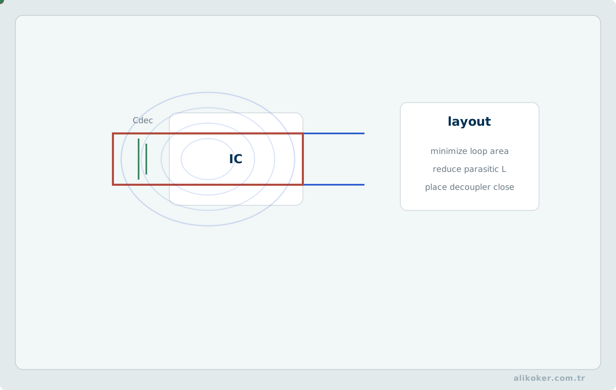
A small capacitor placed close to an integrated circuit's supply pins is used to:
supply sudden current demand locallyand reduce high-frequency supply impedance.
Not only capacitance but also:
- ESR,
- ESL,
- physical placement
matter.
8.25. Grounding and Common Impedance
If two circuits share the same return path, the drop across the common conductor:
v = Zican disturb the reference of the other circuit.
This is a common-impedance coupling problem.
The routing of analog and high-current return paths is therefore important.
8.26. Star Grounding
In some low-frequency systems, joining return-current paths at a single point can reduce common-impedance effects.
However:
“Star grounding is best for every circuit” is not a universal rule.
At high frequency, a broad ground plane may be more appropriate. Grounding should be designed according to frequency and current paths.
8.27. Tolerance Analysis
If a component is specified as:
R = 10 kΩ ±5%its actual value can be:
9.5 kΩ ... 10.5 kΩCircuit output can therefore be examined not only at the nominal value but through:
- worst-case limits,
- statistical distributions.
8.28. Worst-case Analysis
Each component tolerance is selected in the direction that produces the worst output limit.
Advantage:
- a conservative guarantee.
Disadvantages:
- simultaneous extreme tolerances may be improbable,
- the result can be overly conservative.
8.29. Monte Carlo Circuit Analysis
Component values are sampled from probability distributions.
Across thousands of simulations, distributions can be obtained for quantities such as:
- gain,
- cutoff frequency,
- power,
- offset.
This can provide a more realistic view of manufacturing variation.
8.30. Noise
Real resistors and active devices generate noise.
The thermal-noise voltage density of a resistor can be expressed as:
e_n =
√(4kTR)
in V/√Hz.
For a bandwidth B, the approximate RMS noise can be:
v_n =
√(4kTRB)
8.31. Noise Bandwidth
A wider measurement bandwidth collects:
more noise powerTherefore:
Unnecessarily high bandwidth is not always beneficial.
Measurements and analog front ends should generally be limited to the bandwidth actually required.
8.32. Signal Ground and Shielding
Shielding can reduce electric-field interference. For magnetic interference, techniques such as:
- minimizing loop area,
- twisted pairs,
- differential measurement
can be effective.
EMI problems cannot be solved from the schematic alone; physical layout matters.
8.33. Circuit Safety
Electrical hazards are not limited to high voltage. Risk can arise from:
- current through the body,
- short-circuit energy,
- arcing,
- hot components,
- charged capacitors,
- battery fires.
Laboratory work must remain within appropriate safety limits.
8.34. Stored Capacitor Energy
After power is removed, a capacitor can retain:
W = 1/2 CV²of energy.
High-voltage circuits may therefore require:
- a bleeder resistor,
- controlled discharge,
- voltage verification.
8.35. Fuse and Current Limiting
A fuse is a protection element, not a normal functional element of the circuit.
Its purpose is approximately:
unexpected overcurrent
→ interrupt the energy path
Fuse selection depends on:
- rated current,
- time-current characteristic,
- interrupting capacity,
- operating voltage.
8.36. Relationship of Circuit Theory to Other Fields
Circuit theory directly supports areas such as:
Analog electronics
→ op-amps, transistors, filters

Control
→ RLC dynamics, transfer functions

Signal processing
→ Fourier methods, filtering

Power electronics
→ energy, switching, three-phase systems

Communications
→ resonance, two-port networks, spectra

Embedded systems
→ sensors, ADCs, power, digital signal integrity
8.37. Circuit Analysis versus Circuit Design
Analysis:
circuit + values
→ determine behavior
Design:
desired behavior
→ determine topology + values
Design is broader. For example, if:
f_c = 1 kHzis required, merely finding:
RC = 1/(2πf_c)is not enough. Source impedance, load, tolerances, op-amp bandwidth, noise, and standard component values must also be considered.
8.38. When the Measurement Instrument Changes the Circuit
Ideal analysis often assumes measurement has no effect. Real voltmeters, current probes, and oscilloscope probes add resistance, capacitance, and sometimes inductance.
The instrument impedance should be compared with the node being measured. A 10 MΩ input can still load a very high-impedance source, while a few picofarads can dominate at high frequency.
A measurement result is therefore incomplete without its setup: probe type, bandwidth limit, grounding, and sampling configuration are part of reproducibility.
8.39. Circuit Model of a Faraday Cage and Common-Impedance Coupling
Lumped circuit theory does not describe every electromagnetic behavior of a shielded enclosure, but it does model coupling introduced by cable penetrations, shield terminations, and shared return paths. Parasitic capacitance between aggressor and victim, finite shield resistance and inductance, and the input-filter impedance must be considered together. At high frequency even a low-resistance but lengthy grounding conductor can develop appreciable inductive voltage.
Z_connection(f) ≈ R_connection + j 2πf L_connection
v_common = Z_common · (i₁ + i₂ + ⋯)
i_capacitive = C_coupling · d(v₁ − v₂)/dt
Connecting a shield to a reference and providing protective earth are not identical actions. Protective grounding primarily addresses electric-shock safety; high-frequency EMC design concerns the continuity of low-impedance current returns. Removing protective earth is not an acceptable noise-reduction method.
A basic experiment compares victim voltage with and without the shield under equal loading and bandwidth while varying cable orientation, input filtering, and shield termination as separate factors. The lumped model is not a substitute for a full field solution when enclosure shielding effectiveness is required.
8.40. Shielded Cables, Transfer Impedance, and Differential Measurement
A cable braid or foil helps reduce coupling from external fields to signal conductors, but the voltage induced by current flowing on the shield depends on transfer impedance. Cable transfer impedance relates shield current to the voltage induced per unit length in the inner circuit. Connector transitions, bonding points, and seams modify the installed response.
Z_T ≈ V_inner / (I_shield · ℓ)   [Ω/m]
v_differential = v_+ − v_−
CMRR_dB = 20 log₁₀(|A_d / A_cm|)
The first expression presupposes a defined cable geometry and test configuration. Differential measurement can reject common-mode interference, but finite CMRR and unequal source impedances prevent perfect cancellation. The instrument reference may introduce another coupling path. Cable shielding, differential input design, filtering, and physical layout therefore require joint evaluation.
Unit 9: Advanced Modeling, Design Limits, and Engineering Checks
9.1. Historical Development of Circuit Theory
Circuit theory did not appear at a single moment. Important developments can be summarized approximately as:
1800
→ Volta and the electric battery

1820s
→ Ørsted, Ampère, and electromagnetism

1827
→ Ohm: the law relating voltage, current, and resistance

1831
→ Faraday: electromagnetic induction

1845
→ Kirchhoff: node and loop laws

1860s
→ Maxwell: unification of electricity and magnetism in field theory

late 19th century
→ Heaviside: operational methods and transmission-line theory

1880s
→ Thévenin equivalent approach

early 20th century
→ AC power systems, phasor methods, network theory

1920s
→ Norton equivalent and communication-network methods

mid-20th century
→ active circuits, feedback, filter synthesis

after 1970
→ SPICE and computer-aided circuit analysis

present day
→ mixed-signal systems, power electronics, RF, integrated circuits, and numerical simulation
The history of circuit theory is also:
the history of transforming physical systems into more abstract and solvable network models.
9.2. Why Kirchhoff's Laws Remain Fundamental
Transistors, op-amps, computers, and integrated circuits did not exist in Kirchhoff's era.
Yet KCL and KVL still form the basis of modern circuit solvers because they follow from very fundamental physical principles involving:
charge conservation
+
energy relationships
Technology changes; the basis of network equations largely remains.
9.3. Circuits and Graph Theory
Circuit topology can be represented as a graph:
node   → vertex
branch → edge
This makes concepts such as:
- independent KCL equations,
- independent loops,
- incidence matrices,
- spanning trees
systematic.
For computer solution of large networks, topology is as important as algebra.
9.4. Number of Independent Equations
In a connected circuit with N nodes, the number of independent KCL equations is:
N - 1One node is selected as the reference, making one node equation dependent on the others.
This explains why nodal analysis uses N-1 unknown node voltages.
9.5. Relationship Among Branches, Nodes, and Independent Loops
For a connected graph with:
B → number of branches
N → number of nodes
the number of independent fundamental loops is:
L =
B - N + 1
This relation is the topological basis of mesh and loop analysis.
9.6. Linear-algebra View
Solving a circuit often means solving:
A x = bwhere:
A → topology + component values
x → unknown voltages/currents
b → sourcesFor large networks, this makes numerical concepts such as sparse matrices, LU decomposition, and condition numbers important.
9.7. Condition Number
If circuit equations are poorly scaled, a small numerical error can produce a large change in the solution.
For example, a matrix containing values on scales as different as:
1 mΩand:
1 TΩcan be numerically challenging.
Some simulation problems are therefore caused by numerical conditioning rather than circuit physics.
9.8. Thévenin Equivalent with Dependent Sources
For a network containing dependent sources, simply:
turn off sources → combine resistancesis not sufficient.
A correct approach is:
1. Turn off independent sources
2. Keep dependent sources active
3. Apply V_test or I_test at the port
4. R_th = V_test/I_testFor AC networks, the same idea gives:
Z_th = V_test/I_test9.9. Open-circuit and short-circuit Tests
For a linear two-terminal network, if:
V_oc
I_scare known, then:
Z_th =
V_oc/I_sccan be used.
This is especially useful for networks with dependent sources or AC impedances.
9.10. Source Internal Resistance
A practical voltage source can be approximated by:
ideal V_s
+
series R_sA practical current source can be approximated by:
ideal I_s
+
parallel R_sThese are physical applications of the Thévenin and Norton viewpoints.
9.11. A Measurement Instrument Is a Circuit Element
A multimeter or oscilloscope is not merely:
an external object observing the circuit.
During measurement it adds elements such as:
R_in
C_inTherefore correct interpretation requires considering:
measured circuit
+
measurement instrumenttogether.
9.12. Probe Compensation
A 10× passive oscilloscope probe contains a capacitive divider as well as a resistive divider.
Compensation adjusts the:
R ratioand:
C ratioto match.
Incorrect compensation can produce excessive rounding or overshoot on a square wave.
9.13. Sensor Interface Using a Thévenin Equivalent
A sensor output can be modeled as:
V_th
R_thIf the ADC input resistance is:
R_Lthen the measured voltage is:
V_ADC =
V_th R_L/(R_th+R_L)This simple relation explains why a high-source-impedance sensor may require a buffer amplifier.
9.14. ADC Sampling Capacitor
A microcontroller ADC input often contains a sample-and-hold capacitor.
If source impedance is too high, that capacitor may not charge sufficiently during the acquisition interval.
Then:
ADC code
≠
actual input voltagePossible remedies include:
- lower source impedance,
- a buffer op-amp,
- longer acquisition time.
9.15. RC Circuits Are Not Only Filters
RC circuits are used for:
- delay,
- timing,
- debouncing,
- coupling,
- integration,
- ADC anti-aliasing,
- reset generation.
The same relation:
τ = RCcan support many different engineering functions.
9.16. RL Circuits and Power Systems
An inductor:
opposes an abrupt change in currentThis property is fundamental in:
- buck/boost converters,
- motor windings,
- EMI filters,
- current smoothing.
9.17. Flyback Voltage
If current through an inductor is interrupted abruptly:
v = L di/dtcan require a large voltage.
For loads such as relay coils or motors, a:
flyback diodecan provide a safe path for the stored energy.
9.18. Why a Diode Differs from Basic RLC Theory
A diode is nonlinear. Approximately:
i =
I_s(e^(v/(nV_T))-1)Therefore superposition, constant impedance, and a single linear equation system cannot be applied directly.
KCL and KVL, however, remain valid. What changes is the component's v-i relationship.
9.19. Small-signal Linearization
A nonlinear element can be linearized around an operating point as:
i(v)
≈
I_Q
+
g(v-V_Q)where:
g =
di/dv |Qis the small-signal conductance.
Much of transistor-amplifier analysis is based on this idea.
9.20. Large-signal and small-signal Analysis
9.20.1. Large-signal Analysis
The actual nonlinear behavior and movement of the operating point are examined.
9.20.2. Small-signal Analysis
Small variations around an operating point are examined with a linear model.
In an op-amp or transistor circuit:
DC bias analysis and AC small-signal analysis are not the same problem.
9.21. Switched Circuits
In power electronics and digital systems, devices switch between:
ON
OFFstates.
Each switch state may form a separate linear circuit, while the overall system is:
piecewise linearand time-varying.
9.22. Averaged Model
In a high-frequency switched power circuit, slower dynamics can be studied with an averaged model instead of resolving every PWM cycle.
For example, duty cycle:
Dcan be modeled as a control input.
This is one of the areas where circuit theory and control theory directly meet.
9.23. Detecting Errors Through Energy Conservation
If a calculation says:
source supplies 10 W
resistors consume 17 W totalthere is a physical inconsistency.
A rapid check is:
Σp = 0Physical validation should follow algebraic solution.
9.24. Unit Checking
For:
RCthe unit must satisfy:
Ω·F = sFor:
L/Rwe obtain:
H/Ω = sDimensional analysis quickly exposes many incorrect formulas.
9.25. Limiting-case Checks
After deriving a formula, physical behavior should be tested at limits such as:
R → 0
R → ∞
C → 0
C → ∞
ω → 0
ω → ∞For example, for:
H_LP(jω)=1/(1+jωRC)we obtain:
ω→0 → H→1
ω→∞ → H→0which is consistent with low-pass behavior.
9.26. Sign Checking
A calculated result such as:
I = -2 Ais not physically strange. It means:
The actual current flows opposite to the initially chosen reference arrow.
A negative result is often information about the reference direction, not an error.
9.27. Problematic ideal-source Topologies
Connecting two unequal ideal voltage sources directly in parallel:
V1 ≠ V2creates contradictory constraints.
Likewise, two unequal ideal current sources directly in series can be problematic.
In real systems, internal impedances limit the conflict.
9.28. Abruptly Paralleling Capacitors
If ideal capacitors with different initial voltages are connected directly in parallel, the ideal model can imply:
infinite impulsive currentIn reality, ESR, wiring resistance, and inductance limit the current.
This clearly illustrates the physical limits of the ideal circuit model.
9.29. Opening the Current Path of an Inductor
If the path of a current-carrying ideal inductor is opened instantaneously, current continuity would require a very large voltage.
In practice:
- arcing,
- diode conduction,
- parasitic capacitance,
- insulation breakdown
can create a new current path.
Thus an ideal-model result of “infinite voltage” is a physical warning rather than a literal prediction.
9.30. Ideal Lossless LC Circuit
An ideal LC circuit has no energy loss, so oscillation can continue indefinitely.
In a real circuit:
R > 0and energy is dissipated.
The ideal model is:
a limiting case used to isolate the dominant phenomenon in a real system.
9.31. Transition to S-parameters
Two-port z, y, h, and ABCD parameters are useful at low and moderate frequencies.
At high frequency, open- and short-circuit measurements become difficult. RF systems therefore use scattering parameters — S-parameters.
The quantities are defined in terms of:
incident wave
reflected waveThis is one of the gateways from classical circuit theory to transmission-line theory.
9.32. Recognizing the Validity Limits of Circuit Theory
Classical lumped-element models require care when:
- physical dimensions approach the wavelength,
- rise times are very short,
- transmission-line reflections matter,
- EMI/EMC dominates,
- field coupling is significant,
- skin effect and dielectric loss matter.
At that point:
circuit theory
→ electromagnetic-field / transmission-line analysisis needed as a complement.
9.33. Design Workflow
A practical circuit-design workflow can be expressed as:
1. Define the function
2. Define input and output limits
3. Know source and load impedance
4. Select the simplest suitable topology
5. Solve the ideal model
6. Check power and voltage limits
7. Add tolerances
8. Check frequency and transient behavior
9. Add parasitics
10. Simulate
11. Prototype
12. Measure
13. Compare results with the model
14. Update the model or design when necessary9.34. A Concise Approach to Circuit Analysis
If a circuit appears complicated, do not immediately write every possible equation. First ask:
What is being asked?
Which operating regime applies?
DC, AC, or transient?
Which components actually matter?
Can series/parallel reduction be used?
Is nodal or mesh analysis shorter?
Can an equivalent network be used?A good solution is:
not the one using the most formulas, but the one that solves the correct model with the least unnecessary work.
9.35. Order of Evidence in Circuit Analysis
A circuit result should first follow from Kirchhoff laws and component equations, then remain open to an independent cross-check. A nodal-analysis result can be compared with mesh analysis, a Thevenin/Norton equivalent, or numerical simulation.
A simulation model is not the complete physical component. If ESR, parasitic capacitance/inductance, amplifier bandwidth, or supply limits are omitted, the result is valid only under that idealization.
Bench measurements should record source/load impedance, probe loading, and instrument accuracy. Differences among calculation, simulation, and measurement are useful evidence about model assumptions rather than something to hide.
9.36. Transition to Field Models and Shielding Verification
The validity of a lumped equivalent depends on the relation between structure size and wavelength and on the coupling mechanism. When apertures, seams, or cavity resonances dominate, a single RLC network cannot reproduce the spatial field distribution. FEM, FDTD, or integral-equation approaches may then be appropriate, provided mesh resolution, material models, and numerical convergence are documented.
λ = c / (f √εᵣ) (lossless, nonmagnetic approximation)
k = 2π / λHere εᵣ is relative permittivity; the wave number differs for general lossy media. Simulation outcomes should be compared with measurements across aperture sizes, polarization, positions, and frequency. Favorable attenuation at one frequency does not establish broadband protection.
Unit 10: Applications and Circuit Analysis Checklist
10.1. Exercise 1 — Power and Sign
For an element:
v = 12 V
i = -2 Aassume the current reference enters the positive terminal.
Calculate:
p = viand explain whether the result means the element supplies or absorbs power.
10.2. Exercise 2 — Voltage Divider and Loading
For:
V_s = 10 V
R1 = 10 kΩ
R2 = 10 kΩfind the unloaded output.
Then connect:
R_L = 10 kΩCalculate the new output and explain why the loading effect is substantial.
10.3. Exercise 3 — Nodal Analysis
Construct a three-node resistive network.
For the two unknown nodes, derive the matrix:
Gv = iby hand.
Verify the result using:
- hand calculation,
- Python/NumPy,
- SPICE.
10.4. Exercise 4 — Dependent Source
Find the port equivalent of a linear circuit containing a VCCS.
After turning off the independent sources, apply:
V_test = 1 Vand calculate:
I_testThen obtain:
R_th = 1/I_test10.5. Exercise 5 — Maximum Power
Let the Thévenin equivalent be:
V_th = 12 V
R_th = 6 ΩCalculate load power for:
R_L = 1...20 ΩPlot the result and show that the maximum occurs at:
R_L = 6 ΩCalculate the efficiency at the same point.
10.6. Exercise 6 — RC Transient
For:
R = 10 kΩ
C = 100 µF
V_s = 5 Vcalculate:
τ,v_C(τ),v_C(5τ),- initial current.
Design an experiment that could measure the response with an oscilloscope.
10.7. Exercise 7 — Capacitor Initial Condition
A capacitor initially has:
v_C(0-) = 3 Vand a new source is connected at t=0.
First determine:
v_C(0+)from the physical continuity principle.
Then write the complete response using the new steady-state value and time constant.
10.8. Exercise 8 — RL and Flyback
A relay coil has:
L = 100 mH
R = 50 Ωand is driven by:
V = 12 VFind the steady-state current.
Explain why the current cannot fall instantaneously to zero when the switch opens.
Compare simulated cases with and without a flyback diode.
10.9. Exercise 9 — RLC Damping
For:
L = 10 mH
C = 10 µFcompare:
R = 10 Ω
R = R_critical
R = 200 ΩFind:
α,ω0,- the roots,
- the response type.
10.10. Exercise 10 — Phasors
Let:
v(t)=100√2 cos(1000t+30°)and:
Z=10+j10 ΩWrite the RMS voltage phasor. Find the current phasor and the time-domain current.
10.11. Exercise 11 — RC Filter
For a low-pass filter with:
R = 1 kΩ
C = 100 nF- find the cutoff frequency,
- calculate magnitude at
0.1fc,fc, and10fc, - calculate phase,
- plot the Bode response.
10.12. Exercise 12 — Series Resonance
For:
R = 10 Ω
L = 10 mH
C = 1 µFfind:
f0,Q,- bandwidth,
- current at resonance.
Calculate V_L and V_C and show how they can exceed the source voltage.
10.13. Exercise 13 — Power Factor
A single-phase load has:
P = 5 kW
pf = 0.7 lagging
V = 230 V
f = 50 HzCalculate the capacitance required to raise the power factor to:
0.95Compare line current before and after correction.
10.14. Exercise 14 — Transformer
For an ideal transformer:
N1/N2 = 10with secondary load:
Z_L = 8 Ωfind the impedance seen from the primary.
If 20 V RMS is required at the secondary, calculate the primary voltage.
10.15. Exercise 15 — three-phase System
For a balanced Y-connected load:
Z_ph = 10+j5 Ω
V_L = 400 Vfind:
- phase voltage,
- phase/line current,
- power factor,
- total
P, - total
Q.
10.16. Exercise 16 — two-port Network
For a simple T-network, derive:
z11
z12
z21
z22Then cascade two identical T-networks and determine the overall network using ABCD parameters.
10.17. Exercise 17 — Laplace Transient
Apply:
v_s(t)=V_0 u(t)to a series RC circuit.
Write the time-domain differential equation using KCL/KVL. Solve it with the Laplace transform and compare the result with the direct time-domain solution.
10.18. Exercise 18 — RLC with Initial Energy
For an RLC circuit with:
v_C(0-) ≠ 0
i_L(0-) ≠ 0represent the initial conditions as equivalent sources in the Laplace domain.
Separate the total response into:
zero-input
+
zero-statecomponents.
10.19. Exercise 19 — Fourier Series and Filtering
Construct a square wave using Fourier-series terms through the:
1st
3rd
5th
7thharmonics.
For an RC low-pass filter, calculate for each harmonic:
|H(jnω0)|
∠H(jnω0)and reconstruct the output waveform.
10.20. Exercise 20 — op-amp
For an inverting amplifier:
R_in = 10 kΩ
R_f = 100 kΩfind the ideal gain.
Then assume a practical op-amp with:
GBW = 1 MHz
SR = 0.5 V/µsFor a 10 Vpp output, calculate the frequency limits separately from:
- bandwidth,
- slew rate.
10.21. Exercise 21 — Tolerance
For an RC filter:
R = 10 kΩ ±5%
C = 10 nF ±10%calculate the cutoff frequency at:
- nominal values,
- worst-case minimum,
- worst-case maximum.
Then generate its distribution with Monte Carlo analysis.
10.22. Exercise 22 — Measurement Loading
A source has:
V_th = 5 V
R_th = 10 MΩFind the voltage measured by a multimeter with input resistance:
10 MΩCompare it with the ideal-voltmeter result.
10.23. Exercise 23 — Oscilloscope Probe
Suppose a circuit node is driven through:
R_source = 100 kΩCompare the frequency-dependent loading of an oscilloscope modeled as:
1 MΩ || 100 pFand a 10× probe modeled as:
10 MΩ || 10 pF10.24. Exercise 24 — Parasitic Inductance
A switch changes current by:
Δi = 2 Awithin:
10 nsIf the interconnect parasitic inductance is:
L = 20 nHcalculate the possible voltage spike using:
v = L di/dtExplain why PCB layout becomes part of circuit theory at fast edge rates.
10.25. Circuit-analysis Checklist
For each problem, ask:
1. What operating regime applies?
2. Is it DC, AC, transient, or a general signal problem?
3. Are reference directions defined?
4. Is the passive sign convention consistent?
5. Can series/parallel reduction be used?
6. Is nodal or mesh analysis shorter?
7. Are dependent sources present?
8. Are there energy-storage elements?
9. Are initial conditions known?
10. For sinusoids, are RMS and phasor definitions correct?
11. Are impedance signs correct?
12. Is the complex conjugate used correctly in complex power?
13. Is the result dimensionally correct?
14. Is it physically meaningful in limiting cases?
15. Is power conserved?
16. Are real component limits respected?
17. Does the measurement instrument load the circuit?
18. Does the simulation model represent the real circuit adequately?10.26. Conclusion and Quick Formula Summary
10.27. Conclusion
Circuit theory begins with a small set of relations:
i = dq/dt
v = dw/dq
p = vi
v = Ri
KCL
KVLYet this compact core expands into a broad engineering structure:
Resistive networks
↓
Nodal and mesh analysis
↓
Equivalent circuits
↓
Capacitors and inductors
↓
Differential equations
↓
Transient response
↓
Sinusoidal steady state
↓
Phasors and impedance
↓
AC power
↓
Resonance
↓
Magnetic coupling
↓
Three-phase systems
↓
Two-port networks
↓
Laplace and Fourier methods
↓
Filters
↓
Simulation
↓
Laboratory measurementThe most important skill in circuit theory is not memorizing individual formulas.
The essential skill is:
to transform a physical circuit into a model at the correct level of abstraction, select an appropriate analysis method, and validate the result through energy, sign, units, limiting cases, simulation, and measurement.
A circuit solution can look mathematically correct and still be physically wrong.
A simulation can converge perfectly while solving the wrong model.
A measurement can be numerically stable while actually measuring a circuit altered by the instrument itself.
Good circuit engineering therefore proceeds as a closed loop:
Model
↓
Calculate
↓
Simulate
↓
Build
↓
Measure
↓
Compare
↓
Correct the model or designThe final principle is:
Circuit theory teaches ideal elements; engineering requires knowing where the ideal model is no longer sufficient.
10.28. Quick Formula Summary
Current:
i = dq/dt
Voltage:
v = dw/dq
Power:
p = vi
Energy:
w = ∫p dt
Ohm's law:
v = Ri
Conductance:
G = 1/R
Resistor power:
P = I²R = V²/R = VI
Series resistance:
Req = ΣR
Parallel resistance:
1/Req = Σ(1/R)
KCL:
Σi = 0
KVL:
Σv = 0
Capacitor:
i = C dv/dt
Capacitor energy:
Wc = 1/2 Cv²
Inductor:
v = L di/dt
Inductor energy:
Wl = 1/2 Li²
RC time constant:
τ = RC
RL time constant:
τ = L/R
First-order response:
x(t)=x(∞)+[x(0+)-x(∞)]e^(-t/τ)
Sinusoid:
x(t)=Xm cos(ωt+φ)
ω = 2πf
Sinusoidal RMS:
Xrms = Xm/√2
Impedance:
Z = V/I
ZR = R
ZL = jωL
ZC = 1/(jωC)
Admittance:
Y = 1/Z
Series RLC resonance:
ω0 = 1/√(LC)
Complex power:
S = VI* = P+jQ
Real power:
P = Vrms Irms cosφ
Reactive power:
Q = Vrms Irms sinφ
Apparent power:
|S| = Vrms Irms
Power factor:
pf = cosφ = P/|S|
Three-phase power:
P = √3 VL IL cosφ
Ideal transformer:
V1/V2 = N1/N2
I1/I2 = N2/N1
Reflected impedance:
Zin = (N1/N2)² ZL
Transfer function:
H(s)=Y(s)/X(s)
Inductor s-domain impedance:
ZL(s)=sL
Capacitor s-domain impedance:
ZC(s)=1/(sC)
RC low-pass:
H(s)=1/(1+sRC)
Cutoff frequency:
fc=1/(2πRC)References
- Albert-László Barabási. Network Science.
- Alexander, C. K.; Sadiku, M. N. O. Fundamentals of Electric Circuits. McGraw-Hill.
- Celozzi, Salvatore; Araneo, Rodolfo; Lovat, Giampiero. Electromagnetic Shielding. Wiley-IEEE Press, 2008. ISBN 978-0-470-05536-6.
- Dorf, R. C.; Svoboda, J. A. Introduction to Electric Circuits. Wiley.
- Faraday, M. Experimental Researches in Electricity, electromagnetic-induction work, 1830s.
- Franco, S. Design with Operational Amplifiers and Analog Integrated Circuits. McGraw-Hill.
- Haykin, S.; Van Veen, B. Signals and Systems. Wiley.
- Hayt, W. H.; Kemmerly, J. E.; Durbin, S. M. Engineering Circuit Analysis. McGraw-Hill.
- Horowitz, P.; Hill, W. The Art of Electronics. Cambridge University Press.
- Irwin, J. D.; Nelms, R. M. Basic Engineering Circuit Analysis. Wiley.
- Jure Leskovec; Anand Rajaraman; Jeffrey D. Ullman. Mining of Massive Datasets.
- Kirchhoff, G. R. Electrical circuit laws, 1845.
- LTspice Documentation. Analog Devices.
- Maxwell, J. C. A Treatise on Electricity and Magnetism. 1873.
- Nagel, L. W.; Pederson, D. O. “SPICE (Simulation Program with Integrated Circuit Emphasis).” University of California, Berkeley, 1973.
- ngspice Documentation. Open-source SPICE simulator.
- Nilsson, J. W.; Riedel, S. A. Electric Circuits. Pearson.
- Norton, E. L. Equivalent current-source network work, Bell Laboratories, 1920s.
- Ohm, G. S. Die galvanische Kette, mathematisch bearbeitet. 1827.
- Oppenheim, A. V.; Willsky, A. S.; Nawab, S. H. Signals and Systems. Prentice Hall.
- Sedra, A. S.; Smith, K. C. Microelectronic Circuits. Oxford University Press.
- Sundararajan, D. Introductory Circuit Theory. Springer International Publishing, 2020.
DOI: https://doi.org/10.1007/978-3-030-31985-4
- Thévenin, L. Equivalent-generator work, 1883.
- Van Valkenburg, M. E. Network Analysis. Prentice Hall.