


Microprocessors


Microprocessor course notes using the 8085 and 8086 to cover registers, buses, instructions, timing, interrupts, serial/parallel I/O, DMA and memory, extended with RTOS scheduling, interrupt latency, priority inversion, cache/DMA visibility, watchdogs, and deadlines.
Microprocessors provide a compact way to study computer architecture because the relationship between instruction execution, registers, buses, memory, interrupts, and peripheral interfaces is directly visible. The Intel 8085 and 8086 are historically old devices, but many of the architectural concepts they expose remain relevant to embedded systems and modern processors.
Unit 1: Fundamental Concepts
A microprocessor integrates a programmable processing core, including arithmetic/logic, registers, and control logic. In the traditional 8085/8086 distinction, main memory and peripherals are external. Modern microprocessors may integrate caches, memory controllers, interconnects, accelerators, and other system functions.
A microcomputer combines a microprocessor with memory and input/output facilities. A microcontroller integrates the processing core, memory, and peripherals for embedded control.
A processor repeatedly performs:
fetch → decode → executeThe program counter identifies the next instruction. Instruction execution may read operands, modify registers or memory, update status flags, and redirect control flow.
Machine code is the binary representation consumed by the processor. Assembly language provides symbolic mnemonics, labels, expressions, and assembler directives that are translated into machine code.
Unit 2: 8085 Architecture
The 8085 is an 8-bit processor with a 16-bit address bus and a 64 KiB address space.
                 +-------------------+
address/data bus <-> 8085 CPU         |
                 |  ALU              |
                 |  accumulator      |
                 |  registers        |
                 |  PC / SP          |
                 |  control unit     |
                 +---------+---------+
                           |
             +-------------+-------------+
             |                           |
          memory                     I/O devices
Important programmer-visible registers include:
Main programmer-visible registers of the 8085:
- A, 8 bit: Accumulator used as a primary operand and result register for arithmetic and logical operations.
- B, C, D, E, H, and L, 8 bit: General-purpose registers. BC, DE, and HL can also be used as 16-bit register pairs.
- PC, 16 bit: Program counter holding the address of the next instruction.
- SP, 16 bit: Stack pointer identifying the top of the stack.
- Flags, 8 bit: Processor-status register containing Sign, Zero, Auxiliary Carry, Parity, and Carry state.
BC, DE, and HL can be used as 16-bit register pairs. HL is also used as a memory pointer; the symbolic operand M refers to the byte addressed by HL.
The status flags are Sign, Zero, Auxiliary Carry, Parity, and Carry. Flag effects are instruction-specific. INR and DCR do not modify Carry; INX and DCX do not modify flags; DAD affects Carry.
Tracing a processor instruction begins with the program counter, registers, and relevant memory state. During fetch, decode, and execute, identify the datapath used and the state changed. Verification extends beyond the destination register to flags, side effects, and the next instruction address. This separates architectural instruction semantics from cycle-level microoperations.
2.1. Multiplexed address/data Bus
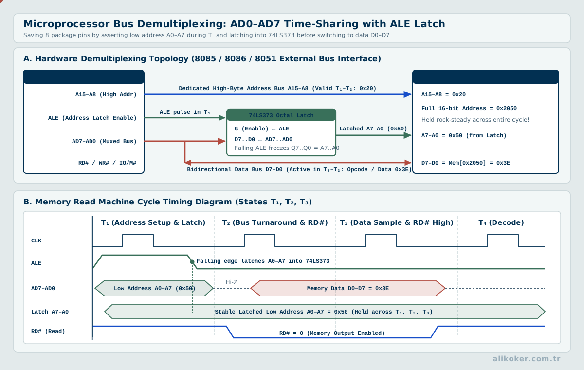
AD0–AD7 carry the low address byte during the first part of a machine cycle and data later in the cycle. ALE allows external hardware to latch the low address. A8–A15 carry the high address byte.
Control signals such as RD, WR, IO/M, S0, and S1 identify bus operations. READY allows slower devices to insert wait states.
2.2. 8085 Register Set, Flags, and Bus Multiplexing
The 8085 exposes the accumulator, general-purpose registers, program counter, stack pointer, and status flags as part of the programmer-visible state. Register pairs such as BC, DE, and HL support 16-bit operations and addressing patterns.
The lower address byte shares pins with the data bus. During the first part of a machine cycle these lines carry address information; later they carry data. The address-latch-enable signal lets external hardware preserve the low address before the bus changes role.
This is a concrete example of a recurring hardware principle: pin count, timing, and external logic are architectural costs that software documentation alone does not expose.
2.3. Addressing Modes as effective-address Rules
Immediate, register, direct, register-indirect, and implied addressing modes describe where an operand comes from and how the effective operand location is obtained.
They should be read together with instruction length and machine-cycle timing. Two instructions that compute the same arithmetic result can generate different bus traffic and latency because they obtain operands differently.
Unit 3: Instruction Set and Addressing
8085 instructions may be one, two, or three bytes long. Multi-byte immediate data and addresses use little-endian byte ordering.
Instruction groups include data transfer, arithmetic, logical operations, branches, stack operations, machine control, and input/output.
Addressing modes include register, immediate, direct, register-indirect, and implied addressing. Understanding the effective address and the number of memory accesses is essential when analyzing timing.
Unit 4: Timing and Machine Cycles
Instruction time is built from T-states and machine cycles. An opcode fetch, memory read, memory write, I/O read, and I/O write have distinct bus behavior.
instruction
  |
  +--> opcode fetch: T1 T2 T3 ...
  |
  +--> memory read/write: T1 T2 T3 ...
  |
  +--> I/O read/write: T1 T2 T3 ...

instruction time = sum of the required machine cycles
A software delay loop derives timing from the exact instruction path:
delay ≈ Σ(instruction T-states) × clock periodBranches make loop timing path-dependent. Interrupts can add jitter, so software delay loops are unsuitable when strict timing must coexist with asynchronous events.
Machine-cycle timing analysis identifies the clock intervals in which addresses and data are valid. Compare read/write-control setup and hold requirements with the attached memory's access time. Recalculate total instruction time if slower peripherals require wait states. Correct logic levels in a timing diagram are insufficient unless validity windows also satisfy physical timing constraints.
From instruction cycles to a real-time budget. In a hypothetical processor clocked at 3 MHz, one T-state lasts 1/3 µs. If a code path requires 30 T-states, its core execution time is 30/3 = 10 µs. If an untaken branch costs 30 states but a taken branch costs 42, worst-case time becomes 42/3 = 14 µs. For a deadline of 12 µs, meeting the average-path budget is not sufficient. Interrupt latency, memory wait states, and peripheral synchronization may need to be included. Validate the cycle counts against the target processor's actual instruction timing table; the figures here are illustrative assumptions, not measured timing for a particular instruction sequence.
Unit 5: Stack and Subroutines
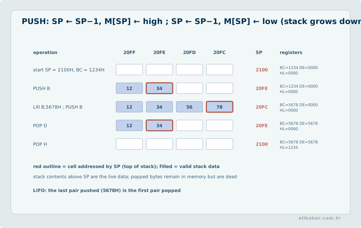
The stack is a LIFO structure addressed through SP. On the 8085 the stack grows toward lower addresses.
CALL saves the return address and transfers control to a subroutine. RET restores the return address. PUSH and POP transfer register-pair data to and from the stack.
Stack correctness depends on balanced operations and valid stack memory. Interrupt handlers and nested calls increase the maximum required stack depth.
Unit 6: Memory and Interfacing
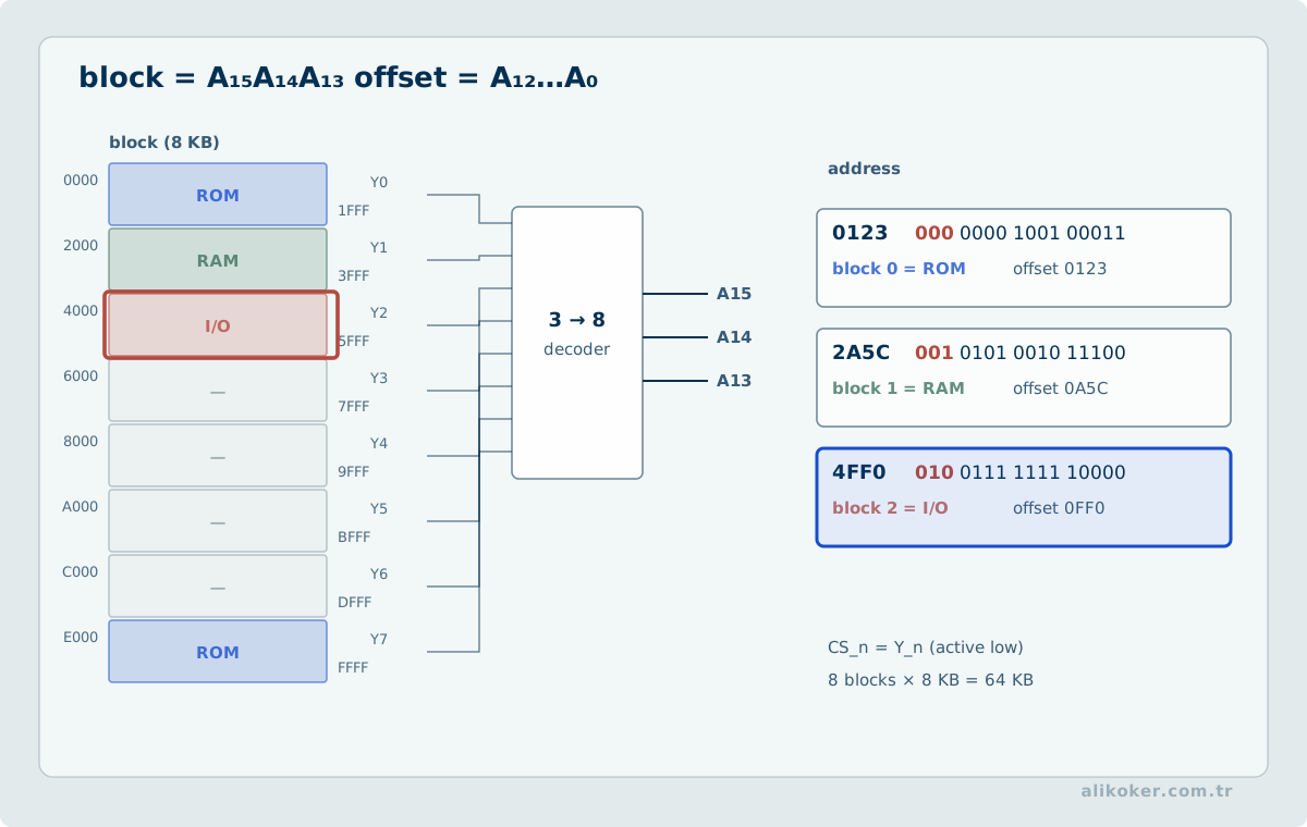
A memory map assigns regions of the processor address space to physical devices. Address decoding determines which chip responds to a bus cycle.
CPU address bus -----+----> RAM
                     +----> ROM
                     +----> memory-mapped I/O

CPU data bus     <---+----> shared data path
CPU control bus  --------> RD / WR / chip select
The 8085 supports isolated I/O through IN and OUT, using an 8-bit port address. Devices may alternatively be memory-mapped, allowing ordinary memory instructions to access them at the cost of consuming memory address space.
Incomplete address decoding can create aliases in which the same physical device responds at multiple addresses.
Unit 7: Interrupts
Polling repeatedly checks device state and consumes processor time. Interrupts allow a peripheral or event to request service asynchronously.
normal program
     |
interrupt request
     |
     v
save current state
     |
     v
run ISR
     |
     v
restore state
     |
     v
resume normal program
The 8085 interrupt inputs include TRAP, RST 7.5, RST 6.5, RST 5.5, and INTR. They differ in priority, maskability, vectoring, and trigger behavior.
TRAP is non-maskable. RST 7.5 is edge-triggered and latched. RST 6.5 and RST 5.5 are level-sensitive. INTR is non-vectored and requires an interrupt-acknowledge exchange.
SIM controls interrupt masks and the serial output function; RIM reads mask, pending-interrupt, global interrupt-enable, and serial-input state.
Interrupt latency is the interval between the request and execution of the handler. Critical real-time systems must account for instruction completion time, higher-priority handlers, masking intervals, and handler prologue overhead.
7.1. Interrupt Structure, SIM/RIM, and Latency
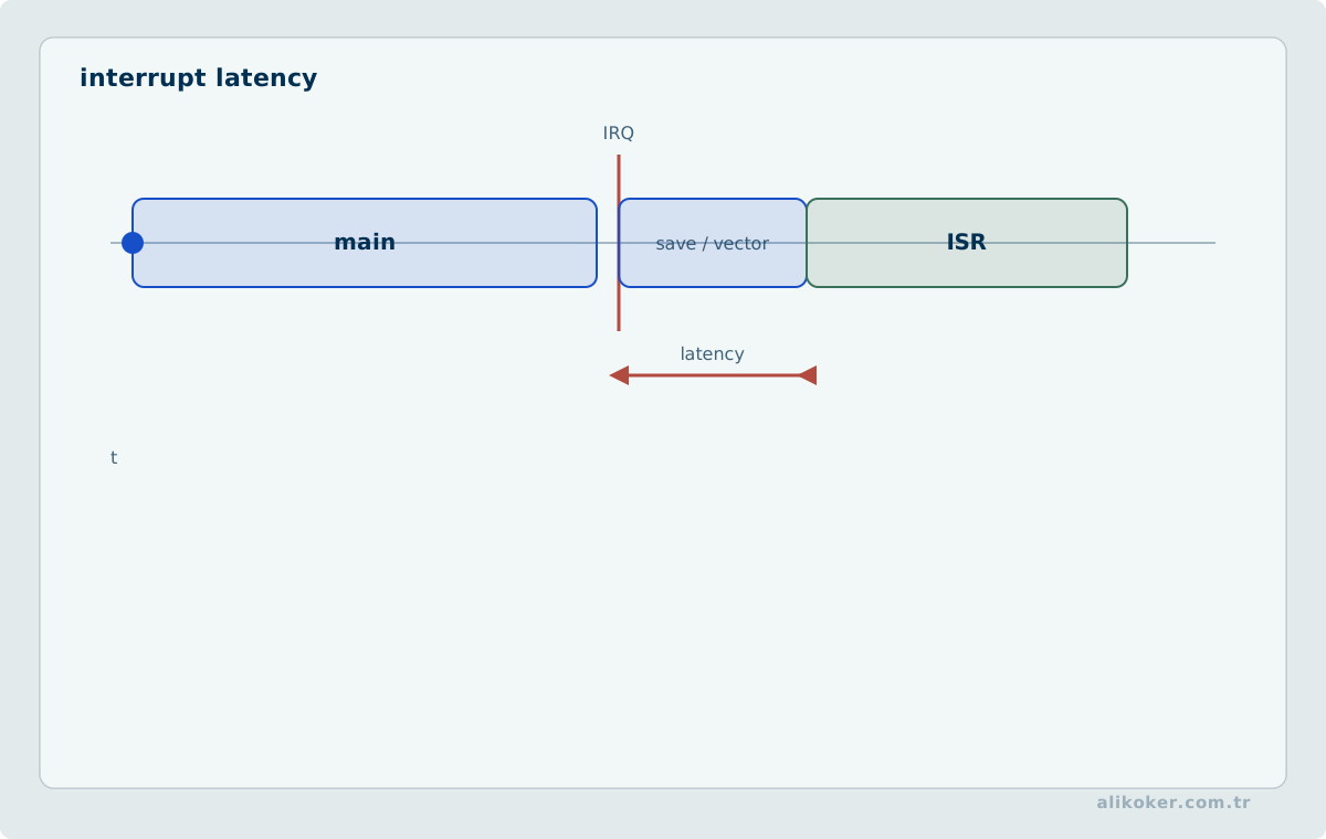
The 8085 interrupt inputs have different priority, maskability, and vectoring behavior. TRAP is non-maskable and highest priority; RST 7.5, RST 6.5, and RST 5.5 are maskable vectored interrupts; INTR requires external interrupt-acknowledge handling.
SIM and RIM expose interrupt-mask and serial-I/O control/status through instructions. Correct use requires understanding which state is latched, which sources are edge- or level-sensitive, and when masks take effect.
Interrupt latency is the time from the external event to useful handler execution. It includes current-instruction completion, recognition, state transfer, vectoring, and handler prologue. For a real-time requirement, worst-case latency matters more than the average.
Unit 8: Serial Communication
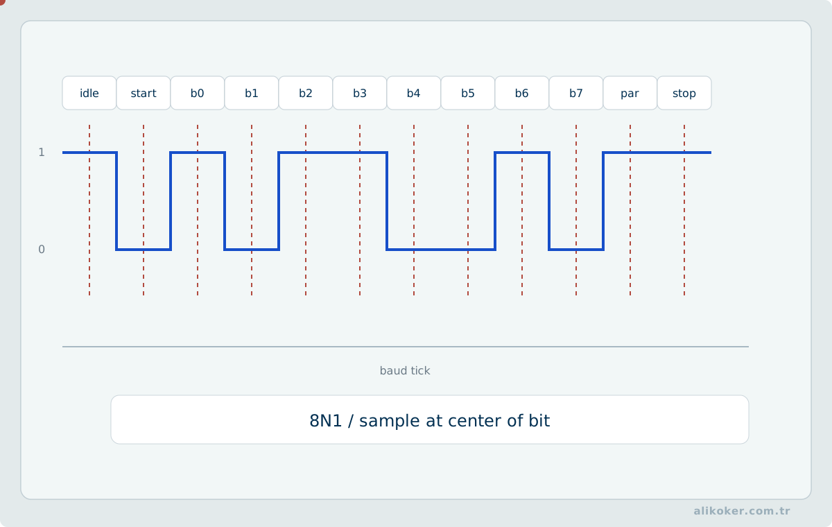
Parallel transfer uses multiple data lines; serial transfer sends bits over fewer lines. Asynchronous serial communication requires an agreed bit rate and framing, typically start, data, optional parity, and stop bits.
The 8085 provides simple SID and SOD pins controlled through RIM and SIM. Software must implement bit timing, so dedicated USART/UART hardware is preferable for reliable communication and lower CPU load.
Electrical standards such as RS-232 define signaling characteristics and should not be confused with higher-level framing or application protocols.
Unit 9: Parallel I/O and the 8255a
The 8255A Programmable Peripheral Interface provides configurable parallel ports.
Its modes support basic input/output and handshaked transfers. Handshaking coordinates producer and consumer when their timing is not inherently synchronized.
The control word determines port direction and operating mode. Correct interface design must consider both logical protocol and electrical loading.
9.1. 8255A Modes and Handshake Semantics
The 8255A provides three ports and programmable operating modes. Mode 0 implements simple input/output. Mode 1 adds strobed I/O with handshake signals. Mode 2 supports bidirectional bus-style transfer on Port A.
Handshake lines exist because the producer and consumer may not be ready at the same time. A status signal turns an electrical transfer into a protocol: data is considered valid only when the required control sequence is satisfied.
This same idea reappears in modern peripheral buses, DMA descriptors, network queues, and asynchronous software pipelines.
Unit 10: Programmable Timers and Counters
The 8253/8254 family provides three independent programmable 16-bit counters. Each channel has clock, gate, and output signals.
Operating modes support terminal count, rate generation, square-wave generation, hardware-triggered strobes, and related timing functions. The 8254 adds read-back functionality.
Hardware timers provide more deterministic timing than processor delay loops because the counter progresses independently of ordinary instruction execution.
Unit 11: Data Transfer Schemes
11.1. Programmed I/O
The CPU explicitly polls and transfers each data item. The design is simple but wastes processor cycles.
11.2. Interrupt-driven I/O
The device interrupts when service is required. CPU utilization improves, but every transfer still involves interrupt and software overhead.
11.3. Direct Memory Access
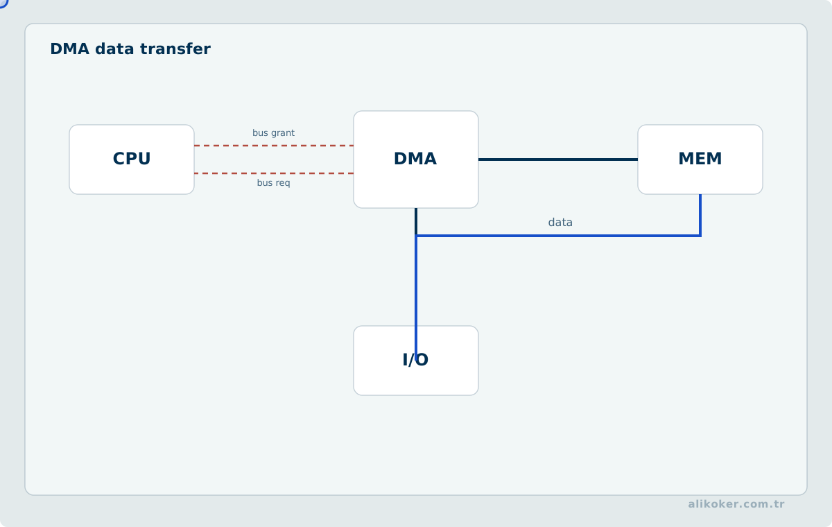
DMA transfers data between a peripheral and memory without routing every data word through ordinary CPU instructions. On classic bus-based systems a DMA controller requests bus ownership with HOLD, and the processor acknowledges with HLDA.
DMA improves throughput for block transfers but introduces bus arbitration, cache-coherency, ordering, buffer ownership, and synchronization issues in modern systems.
Unit 12: 8086 And the Transition to 16 Bits
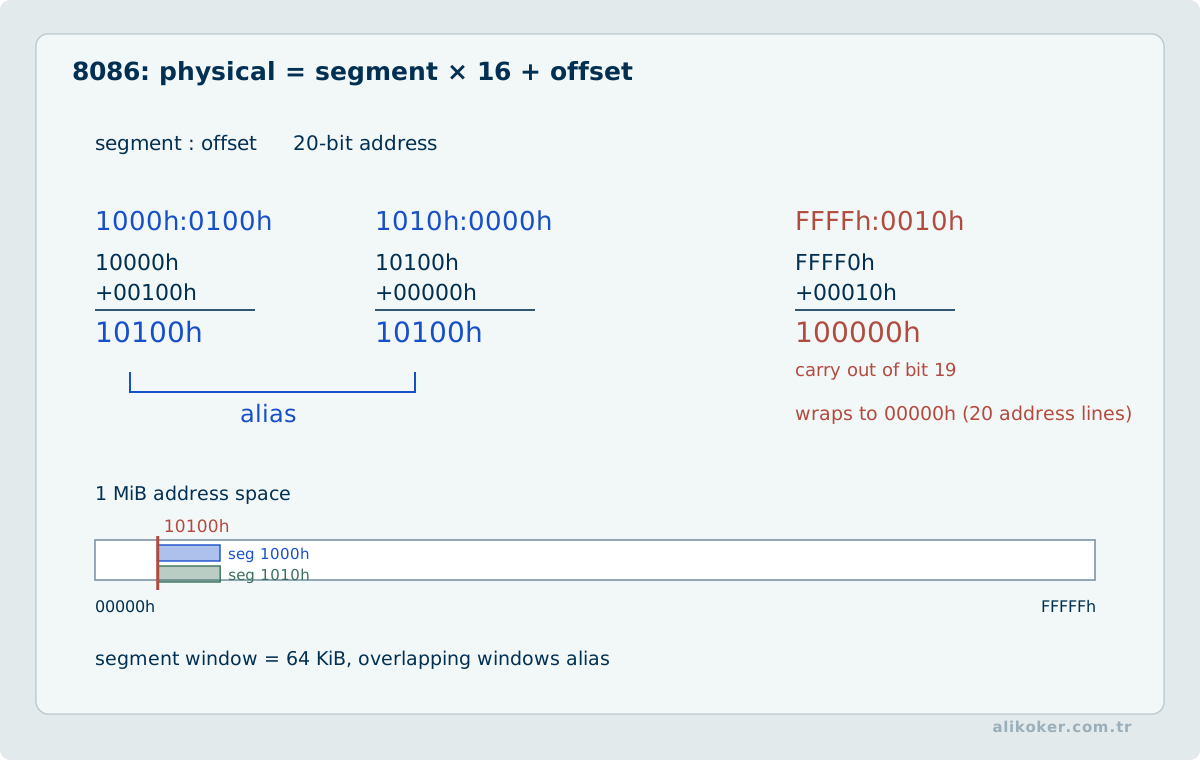
The 8086 has a 16-bit data path and a 20-bit address space. Its Bus Interface Unit and Execution Unit allow instruction prefetch to overlap with execution.
Segment registers CS, DS, SS, and ES participate in physical address formation:
physical address = segment × 16 + offsetThe segmented model allows a 16-bit offset to participate in addressing a 1 MiB physical space, but creates aliasing and software complexity.
String instructions use SI, DI, and the Direction Flag. REP prefixes repeat operations under control of CX.
12.1. 8086 Segmentation and the Transition to Wider Systems
The 8086 separates execution and bus-interface responsibilities and introduces a segmented address model. A physical address is formed conceptually from a segment base and an offset:
physical = segment * 16 + offset.
Code, data, stack, and extra segment registers select conventional segment bases. The scheme extends addressability beyond one 16-bit offset, but also creates aliasing: different segment:offset pairs can identify the same physical location.
The 8086 transition is useful not only historically. It shows how an architecture can extend address space while preserving compatibility constraints, and why later protected and flat address models changed the programming contract.
Unit 13: Classical Concepts in Modern Architectures
13.1. CISC and RISC
CISC and RISC describe design tendencies rather than a strict modern binary classification. Contemporary processors often decode complex architectural instructions into simpler internal operations.
13.2. Pipelining
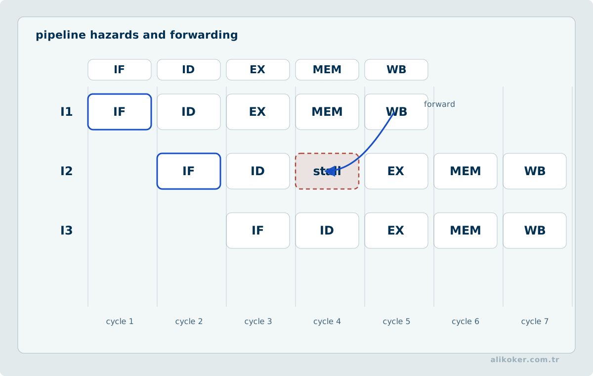
Pipelining overlaps stages of different instructions. Ideal throughput is limited by data, control, and structural hazards. Forwarding, speculation, branch prediction, out-of-order execution, and duplicated resources mitigate these hazards but increase complexity.
For hard real-time systems, mechanisms that improve average throughput can complicate worst-case execution-time analysis.
13.3. Cache and Memory Hierarchy
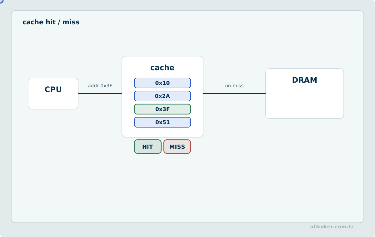
Modern systems bridge the latency gap between CPU and main memory using multiple cache levels. Locality is therefore a performance property of software as well as hardware.
13.4. Interrupt Controllers and DMA
Modern interrupt controllers support prioritization, routing, affinity, and large interrupt spaces. DMA engines support scatter/gather, circular buffers, peripheral triggers, and memory-to-memory transfers.
13.5. Protection and Security
Privilege levels, memory protection, MMUs/MPUs, execute permissions, isolation, and virtualization extend the simple memory-map concept into system-wide protection mechanisms.
13.6. Multicore Systems
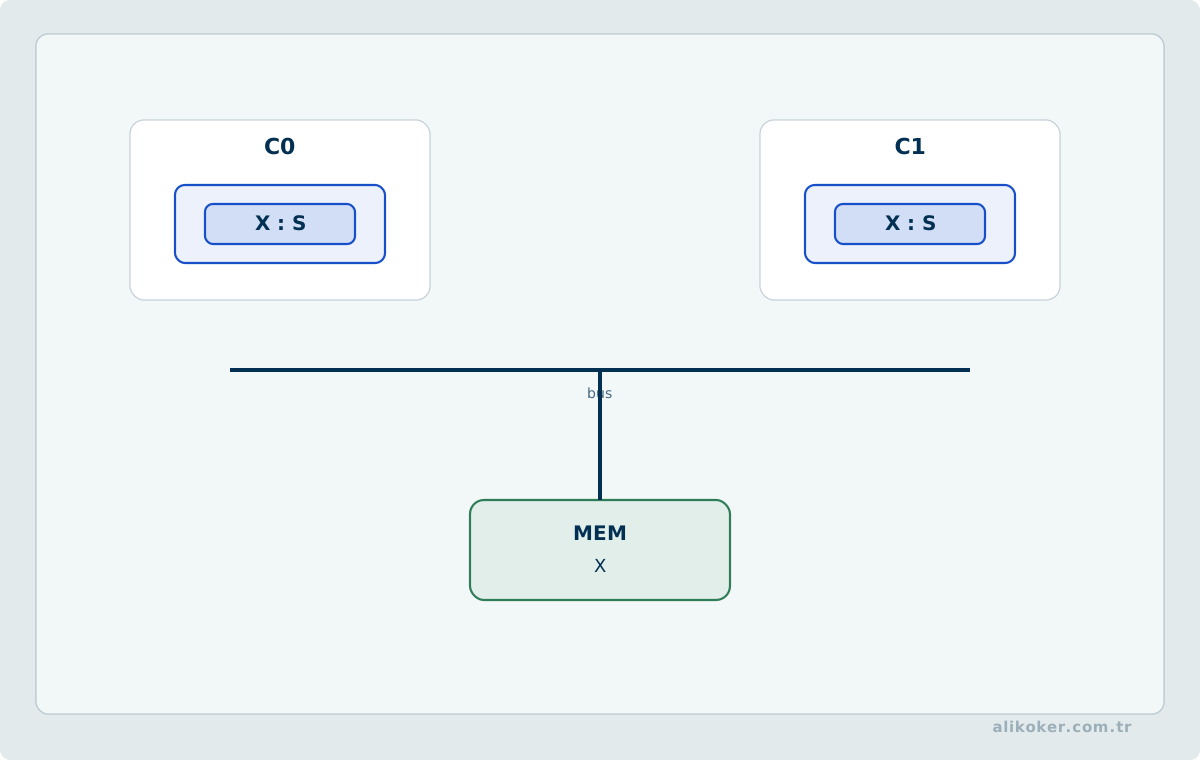
Multiple cores introduce concurrency and memory-consistency concerns. Cache coherence, atomic operations, memory ordering, locks, and lock-free algorithms become part of processor-level programming.
13.7. Watchdogs, Timeouts, and Safe State
In a modern embedded system it is not enough for the processor to execute correct instructions; the design also needs a way to detect when software stops making progress or exceeds a required time bound. A hardware watchdog timer can reset the processor or initiate a recovery action when software fails to provide an expected liveness indication within the configured interval.
A watchdog is not fault tolerance by itself. The design must define output state after reset, handling of partially completed operations, prevention of endless restart loops after persistent faults, and the path to a safe or degraded state. The flight-computer and critical real-time context is extended in Avionics Systems and Unmanned Aerial Vehicles.
13.8. Real-Time Behavior on MCU/SoC Systems
Interrupts, timers, DMA, and memory-mapped I/O from the classical microprocessor model form the basis of real-time software on modern MCUs and SoCs. A fast processor, however, is not the same thing as predictable timing.
13.8.1. Interrupt Latency
The delay between an interrupt event and the beginning of its ISR is not determined by clock frequency alone. Higher-priority interrupts, interrupt-masked regions, pipeline/cache state, and operating-system critical sections can all contribute.
event
 ↓
interrupt pending
 ↓
safe interruption of current work
 ↓
context save
 ↓
ISR start
For real-time design, a defensible upper bound is more useful than average interrupt latency.
13.8.2. RTOS Tasks and Priority
An RTOS scheduler can run periodic or event-driven tasks according to priority. High priority should not simply mean "important code"; it should follow deadlines and dependency structure.
When tasks share locks, priority inversion may occur. Priority-inheritance or priority-ceiling protocols can be used to bound this form of blocking.
13.8.3. Cache, DMA, and Visibility
A DMA engine accesses memory independently of the CPU. On a cached SoC, the following mismatch can occur:
new data in CPU cache
old data in RAM
DMA reads RAM
The reverse can also happen when DMA writes new data that remains hidden behind a stale CPU cache line.
Cache maintenance, memory barriers, and DMA-buffer rules must therefore follow the platform contract. volatile is not a cache-coherency mechanism; it constrains compiler treatment of accesses but does not by itself synchronize hardware caches.
13.8.4. Watchdogs and Deadlines
A watchdog should not answer only "is the program stuck?" Feeding it without proving forward progress can hide a system that is alive at instruction level but dead at functional level.
A stronger pattern is:
critical tasks made progress?
        ↓ yes
health aggregation
        ↓
watchdog service
13.8.5. Predictability Budget
A real-time path may contain:
sensor interrupt
+ ISR
+ queue/wakeup
+ task execution
+ bus/DMA
+ actuator update
The combined worst-case delay must remain below the deadline. Adding average times does not create a real-time guarantee.
This provides the natural bridge from microprocessor mechanisms to a separate course on embedded and real-time systems while keeping the hardware roots visible here.
13.9. The Cost of Data Movement in Microprocessors
In a microprocessor-based controller, the data path to peripherals can matter as much as arithmetic speed. DMA transfers, interrupt-service latency, cache-maintenance requirements, and memory mapping all affect sampling-loop timing. A timing analysis should include bus contention, the points at which transfers start and complete, and real-time interrupt priorities rather than relying only on instruction counts.
- Compare latency and energy costs across the register-cache-DRAM hierarchy.
- Classify pipeline stalls into branch, dependency, and memory-wait causes.
- Relate performance-counter evidence to source-level access patterns.
Unit 14: Portability and Verification at the Hardware-Software Boundary
Classical microprocessor study focuses on registers, instructions, buses, and peripherals. Reliable modern embedded software must also respect the contracts among the processor, compiler, ABI, memory system, and device interfaces.
14.1. Endianness and Data Representation
Endianness defines the byte order used to store a multibyte value in memory. The numerical value does not change; its physical byte representation does. The distinction becomes visible in binary file formats, network protocols, peripheral registers, and data exchange across architectures.
Portable code should implement the byte order specified by the protocol or file format instead of assuming the host representation. The same caution applies to C and C++ bit-fields: their language-level layout should not be assumed to match a hardware register map automatically.
14.2. Alignment and Access Width
Natural alignment affects where a processor can access a value efficiently or, on some architectures, legally. An unaligned access may be handled in hardware, split into multiple memory transactions, or raise a fault depending on the ISA and system configuration.
Packed network or file data should therefore not be converted blindly into a pointer to a wider integer type. Data representation, alignment, and language aliasing rules must be considered separately from the electrical bus width.
14.3. ABI and Calling Conventions
The instruction set architecture defines the available machine-level operations. An application binary interface (ABI) defines how separately compiled components interact: where parameters are passed, where return values appear, which registers are caller- or callee-saved, and how the stack is aligned.
More than one ABI can exist for the same ISA. Assembly/C/C++ boundaries therefore require the target ABI specification in addition to the processor manual.
14.4. Address Translation and Protection Boundaries
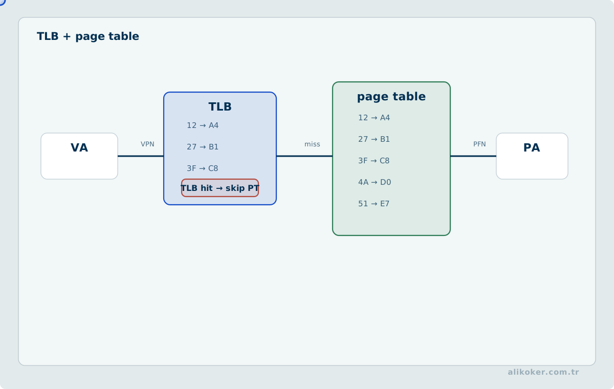
A small microcontroller may expose a direct physical memory map. Larger systems can use an MMU to translate virtual addresses to physical addresses, while an MPU can enforce region-based access permissions. These mechanisms are related but not interchangeable.
Keep these distinctions explicit:
virtual address != physical address
access permission != cache policy
privilege level != user identity
address mapping != ownership
An address being valid does not imply that the access is low latency, cacheable, or safe for every execution context.
14.5. DMA, Caches, and Ownership
A DMA engine accesses memory independently of the CPU, creating two potential actors over the same buffer. On cached systems, sharing a pointer does not by itself guarantee visibility. The platform may require cache maintenance, memory barriers, an ownership protocol, or hardware-coherent DMA.
A robust buffer protocol makes ownership explicit:
CPU prepares buffer
        ↓
ownership transferred to DMA
        ↓
DMA transfer
        ↓
completion event
        ↓
CPU owns buffer again
This prevents ambiguous simultaneous modification of the same storage.
14.6. Hardware Counters and Measurement
Source-line count or instruction count is not execution time. Cache misses, branch prediction, wait states, bus contention, and interrupts can change cycle counts.
When available, cycle counters and performance-monitoring facilities can be combined with external techniques such as oscilloscopes, logic analyzers, or GPIO timing markers. Instrumentation itself has cost, so the measurement method must be part of the experiment description.
14.7. ISA, ABI, and Microarchitecture Are Different Layers
A useful separation is:
ISA           → programmer-visible instruction and state contract
ABI           → binary calling and data-layout contract
microarchitecture → hardware implementation of those contracts
Two processors implementing the same ISA may use very different pipelines, caches, predictors, or execution units. Functional portability therefore does not imply timing portability.
14.8. Reading the Microprocessor Through Instructions, Datapaths, and Peripheral Timing
A microprocessor system can be understood as three components connected through three classes of signals: the processor, memory, and input/output devices. The address bus answers where, the data bus answers what, and the control bus answers when and in which direction. Most topics in this course are concrete forms of these three questions.
Addressing is a decoding problem. Memory-chip selection, I/O-port selection, and segmentation all partition an address so that some bits identify a target while the remaining bits identify a location within that target. Modern address translation adds more layers, but the underlying separation between target selection and offset remains.
Timing is a synchronization problem between components with different speeds and timing contracts. Wait states, handshaking, buffering, caches, interrupt latency, DMA arbitration, and peripheral timing requirements are different mechanisms for reconciling those mismatches. Correctness therefore depends not only on logical values but also on when signals and data become valid.
Control transfer is a context-preservation problem. A subroutine call, an interrupt, and a task switch are progressively broader versions of the same pattern: preserve enough execution state, transfer control, perform work elsewhere, and restore the state required to continue. Incorrect stack or context management can corrupt all three forms.
Data transfer can be ordered by how much processor participation it requires. Programmed I/O keeps the processor directly involved; polling adds explicit readiness checks; interrupts let the device request service; DMA moves bulk data with substantially less per-word CPU participation. Moving along this spectrum reduces direct CPU work but increases hardware, synchronization, ownership, and visibility concerns.
The enduring value of the 8085 and 8086 material is that these principles are visible without the additional layers of a modern processor. Pipelining, caches, virtual memory, privilege levels, multicore coherence, memory ordering, and system-on-chip interconnects do not replace the classical model; they build additional machinery on top of the same fundamental contracts among execution, storage, and I/O.
14.9. Core Architecture and Execution Concepts in a Microprocessor
The enduring architectural chain is:
instruction
→ registers
→ datapath
→ bus transaction
→ memory or peripheral
→ timing
→ interrupt/DMA interaction
→ system-level concurrency
Studying classic processors is useful because these mechanisms are visible without the layers of speculation, cache hierarchy, and out-of-order execution present in modern high-performance CPUs.
14.10. Memory-mapped I/O, volatile, And Hardware Ordering
Peripheral registers mapped into memory do not behave like ordinary RAM. Reads and writes can have device side effects, and values can change independently of the program.
In embedded C/C++, volatile helps ensure accesses are emitted, but it does not provide thread-safe atomicity or a CPU memory barrier. Multicore systems and DMA-shared buffers may require architecture-specific ordering rules.
Register definitions must respect read-only, write-one-to-clear, and reserved bits. A naive read-modify-write can accidentally clear unrelated status flags.
14.11. Verifying Code Against the Datasheet
A peripheral register needs more than a bit name. Reset values, access type, reserved-bit behavior, and semantics such as write-one-to-clear should be checked against the device documentation.
Oscilloscope or logic-analyzer measurements can verify whether physical timing matches the intended software sequence. Interrupt latency, bus speed, and DMA interaction cannot be inferred from source-code line count.
Examples from 8085/8086, ARM, and RISC-V should not be generalized across architectures. ISA rules, vendor MCU documentation, and board-level electrical limits are separate reference layers.
14.12. From Microprocessors to Edge AI Inference
The strongest connection between microprocessors and AI appears when a learned model must run on a resource-constrained device. Unlike a server, an embedded target has simultaneous limits on RAM, flash, execution time, and energy. Edge AI is therefore not merely model compression; it is the problem of mapping an algorithm onto real microprocessor constraints.
A simple inference path is:
sensor / input
↓
preprocessing
↓
model
↓
decision
↓
output / actuator
Every stage consumes time and memory. Weights may reside in flash while selected data are moved into SRAM. If intermediate tensors need not coexist, buffer reuse can reduce the memory peak.
Quantization is central. Converting FP32 weights and activations to INT8 or narrower forms can reduce storage and arithmetic cost, but scale, zero point, rounding, and saturation become part of numerical behavior. Post-training quantization may reduce quality; quantization-aware training can model the error during training. The actual gain must be measured on the target device.
Fixed-point arithmetic makes classical microprocessor concerns visible again: multiplication width, overflow, saturation, and rounding can change model output. The real cost also depends on DSP/SIMD instructions, memory behavior, and available inference kernels.
Real-time behavior matters when sensor samples arrive periodically. Average inference time is not sufficient if worst-case latency misses the acquisition deadline. DMA and double buffering can help move continuous sensor data without unnecessary CPU copies.
Energy is an independent metric. Lower latency does not automatically mean lower energy; task energy depends on clock, memory traffic, and power state.
Microprocessor theory does not explain how the model learns. It explains how a learned function becomes an embedded task with bounded memory, time, data movement, and energy.
14.13. Following an Instruction Through the Hardware
Instead of learning microprocessors as disconnected lists of registers and instructions, following one instruction through execution connects several concepts at once. The processor fetches the instruction addressed by the program counter, decodes the opcode, obtains operands from registers or memory, performs the operation, and writes the result to its destination. The program counter, flags, address and data buses, and control signals are different parts of that same execution.
Consider an abstract instruction such as LOAD R1, [A]. The instruction itself must first be fetched. The address A is then generated, a memory-read transaction takes place, and the returned data is written into R1. If memory and processor timing differ, wait states or cache behaviour can affect the elapsed time. Statements such as “one instruction takes one cycle” therefore cannot be generalized without separating the instruction-set architecture from its microarchitectural implementation.
Polling, interrupts, and DMA solve different versions of the same I/O problem. Polling repeatedly asks whether a device is ready. An interrupt allows a device to redirect processor execution to a handler when service is required. DMA reduces the need for the CPU to move every individual word during a larger transfer. None is universally superior; transfer size, latency requirements, interrupt overhead, and available hardware support matter.
Endianness is likewise about byte ordering rather than numerical value. The same multibyte value may be stored in different byte orders; the value is unchanged while its physical representation changes. This distinction becomes visible when working with network protocols, binary files, or peripherals.
A useful way to read a microprocessor problem is therefore as an address generation -> data movement -> operation -> state change chain. That chain also forms the bridge to Computer Architecture and embedded-system design.
14.14. Peripherals, Serial Buses, and Timing Contracts
Programming a microprocessor or microcontroller is not only about knowing the instruction set. In a real system, the processor interacts with sensors, motor drivers, converters, communication modules, and other controllers through peripheral registers and physical buses. This layer connects a microprocessor course to embedded-system design.
14.15. GPIO: a Digital Pin Is More Than Zero and One
A GPIO pin may expose separate controls for direction, pull-up or pull-down configuration, drive strength, edge detection, and alternate functions. Writing 1 to a register does not guarantee an ideal logic level under every physical condition; load, voltage domain, rise/fall time, and electrical limits must be verified from the device datasheet.
14.16. UART, SPI, and I²C Implement Different Communication Contracts
UART is asynchronous serial communication. It carries no shared clock line, so both endpoints must agree on baud rate, data bits, parity, and stop-bit configuration. It is simple and common for continuous byte streams.
SPI is a synchronous master/peripheral interface driven by a shared clock. Separate clock and data lines can support high transfer rates, while multiple peripherals require chip-select management. The interface itself does not define an application-level message format.
I²C is an addressed bus on which many devices can share clock and data lines. Open-drain signaling and pull-up resistors are part of its physical behavior. Start, stop, ACK/NACK, and addressing rules define the transfer contract.
UART   TX ───────── RX       asynchronous, mostly point-to-point
       RX ───────── TX

SPI    SCLK ───────┬────     shared clock
       MOSI ───────┼────     separate data paths
       MISO ───────┼────
       CS0/CS1 ────┴────     device selection

I²C    SCL ────────┬────     shared clock
       SDA ────────┴────     shared addressed data
For these buses, “the protocol works” means more than observing the expected bytes. Clock rate, trace or cable capacitance, pull-up values, voltage levels, chip-select timing, and setup/hold constraints in the datasheet all matter.
14.17. Polling, Interrupts, and DMA Solve the Same Problem with Different Costs
Continuously checking a peripheral with polling is simple but consumes CPU time. An interrupt notifies the processor when an event occurs and can be more efficient at low event rates, while interrupt storms and priority behavior become design concerns. DMA can move large or regular blocks without CPU involvement for every byte, but buffer ownership and cache visibility then require explicit attention.
polling   → CPU waits and asks repeatedly
interrupt → the device event invokes CPU handling
DMA       → device/memory transfer proceeds in blocks
The choice is not based only on average throughput. Worst-case latency, CPU budget, energy consumption, and risk of data loss are also design variables.
14.18. Real Time Means Proving a Timing Bound, Not Merely Being Fast
Average execution time is insufficient for an embedded task. Worst-case execution time (WCET), interrupt latency, priority, blocking on shared resources, and the aggregate CPU demand of periodic tasks must be evaluated together with deadlines.
sensor sampling period : 10 ms
deadline               : 10 ms
WCET                    : 2.4 ms
interrupt/blocking budget: 0.8 ms
remaining timing margin: 6.8 ms
These values are only an illustrative budget; real WCET and jitter require measurement or an appropriate analysis method. An RTOS provides task priorities, scheduling, and synchronization mechanisms, but it does not make a system deterministic by itself. Long critical sections, priority inversion, cache misses, DMA interference, or blocking driver calls can still violate a deadline.
14.19. A Watchdog Constrains a Failure Model; It Does Not Repair the Bug
A watchdog timer can detect the absence of progress within a configured interval and trigger a reset or safe-state transition. Feeding the watchdog unconditionally from a periodic timer can make a deadlocked system appear healthy. The feed decision should therefore depend on a health condition that demonstrates progress in the critical tasks.
This is where the distinction between a microprocessor and an embedded system becomes clear: the processor executes instructions, while the embedded system must ensure that those instructions produce the correct result within physical, energy, timing, and failure constraints.
Unit 15: Startup, Interrupts, and Peripheral Timing in Modern Cortex-M Microcontrollers
The classical 8085/8086 model remains valuable because instruction cycles, buses, interrupts, and peripheral interfaces still exist in modern systems. In a contemporary microcontroller, however, these ideas are integrated through reset vectors, an interrupt controller, a clock tree, pin multiplexing, timers, data converters, and DMA. This section is not a programming guide for a particular STM32 device. Its purpose is to establish a portable engineering model for reading Cortex-M device data sheets and reference manuals.
15.1. Reset, Startup Code, and the Vector Table
Execution after reset should not be reduced to "main is called." A typical path is:
reset
  ↓
initial stack pointer from vector table
  ↓
reset-handler address
  ↓
clock / memory / runtime initialization
  ↓
copy .data and clear .bss
  ↓
prepare C/C++ runtime
  ↓
main
The vector table contains handler addresses for core exceptions and peripheral interrupts. Linker scripts, startup files, and interrupt-handler symbols therefore form one execution contract. A wrong section placement or mismatched handler name can produce a reset loop or entry into a default handler even when the source code compiles successfully.
15.2. NVIC, Exceptions, and Priority
The Cortex-M Nested Vectored Interrupt Controller (NVIC) manages interrupt enable state, pending/active state, and priorities in close integration with the processor core. Priority is not merely a number. A design must answer:
- which event has which deadline?
- may one handler preempt another?
- how long can a critical region mask interrupts?
- how are equal-priority events ordered?
- does a handler perform blocking work?
- how is shared state protected?
An unnecessarily long high-priority handler can starve a lower-priority but timing-critical peripheral. Interrupt-driven software is not automatically deterministic; interrupt latency + handler WCET + preemption + blocking must fit a timing budget.
15.3. Clock Tree and SysTick
A microcontroller can expose one advertised CPU frequency while peripherals operate from different clock domains. Oscillator/RC sources, PLLs, selectors, and prescalers can derive separate clocks for the core, buses, timers, UARTs, or ADC blocks.
clock source
   ↓
PLL / selector
   ↓
prescaler
   ├─ core clock
   ├─ peripheral bus A
   └─ peripheral bus B
Baud-rate and timer calculations must use the clock that actually reaches the peripheral, not an assumed CPU clock. Clock changes can also affect flash wait states, power consumption, and peripheral timing.
SysTick is a Cortex-M system timer commonly used as an operating-system tick or a simple time base. It is not necessarily the best mechanism for high-resolution measurement; timer capture, a cycle counter, or a dedicated hardware timer may provide a more appropriate clock. A tick-based software delay should not be interpreted as absolute timing accuracy.
15.4. GPIO and alternate-function Routing
Modern MCU pins are usually multiplexed. One physical pin can act as GPIO, UART, SPI, a timer channel, or an analog input. Correct operation therefore depends on several independent configuration decisions:
pin mode
+ alternate-function selection
+ electrical drive / pull-up / pull-down
+ peripheral clock and peripheral configuration
Push-pull versus open-drain, internal pulls versus external resistors, and output slew settings are distinct concerns. For buses such as I²C, the electrical topology is part of protocol behavior.
15.5. Timers as Timing Contracts
General-purpose timers do more than generate periodic interrupts. Prescalers and counter periods establish a time base, while channel logic measures external events or generates outputs.
Input capture latches the counter on an input edge, allowing period or pulse-width measurement without software polling. Output compare generates an event when the counter reaches a programmed value. PWM uses timer hardware to define period and duty cycle.
counter clock = timer clock / prescaler
period ticks  = auto-reload + 1
PWM duty      = compare / period ticks
These expressions are conceptual. Device-specific details such as timer-clock multiplication, center-aligned modes, or shadow registers must be verified in the reference manual.
15.6. ADC, DAC, and the Sampling Chain
ADC resolution is not the same as measurement accuracy. Reference voltage, source impedance, sample-and-hold time, quantization, offset/gain error, noise, and PCB layout all influence the result.
For an ideal N-bit ADC, the code range is approximately 0 ... 2^N - 1, but nominal LSB size is not a guarantee of real-world precision. If the sampling interval is too short for a high-impedance source, the internal sampling capacitor may not settle sufficiently.
A DAC converts a digital code into an analog level; settling time, output drive, and load still matter. Generating an analog-like level by filtering PWM is a different design from using a true DAC.
15.7. DMA as a Transfer Engine and Ownership Protocol
DMA is not only a CPU-offload feature. It can maintain peripheral data flow with lower scheduling jitter, but it introduces an explicit buffer-ownership problem:
CPU fills buffer
   ↓
ownership moves to DMA
   ↓
DMA transfers
   ↓
completion event
   ↓
ownership returns to CPU
Double buffering or circular DMA can sustain continuous acquisition, but an imbalance between producer and consumer rates still causes overwrite or underrun. On MCU/SoC designs with caches, CPU and DMA visibility can require cache maintenance and memory-ordering rules. volatile alone does not solve cache-coherency or ownership problems.
15.8. Register Access, CMSIS, and HAL
The same hardware can be controlled through multiple abstraction layers:
application
  ↓
vendor HAL / driver
  ↓
CMSIS and device header
  ↓
register / memory-mapped I/O
  ↓
hardware
Register-level code can provide precise control and predictable hot paths but increases portability and maintenance cost. A HAL can accelerate development while potentially introducing polling, timeout logic, or additional state transitions that must be measured in timing-critical paths. An abstraction layer is a contract to verify, not a performance assumption.
Reliable embedded design therefore does not choose one layer ideologically. It uses the lowest abstraction level justified by deadline, power, memory, safety, testability, and maintenance requirements.
15.9. Counter Overflow and Missed Edges in Encoder Capture
A free-running 16-bit timer clocked at 1 MHz wraps every 65536 µs = 65.536 ms. If two encoder edges are separated by 80 ms, directly subtracting raw counter values may produce an incorrect interval. Overflow events must be accounted for or a wider time base used. With 20 kHz of edge events, mean separation is 50 µs; a lengthy software interrupt on every edge can consume the latency budget of unrelated tasks.
Hardware input capture can timestamp an edge before its interrupt service begins. DMA transfer into a ring buffer can lower CPU interrupt overhead, but ring overflow, producer–consumer ownership, and cache visibility then become correctness concerns. A hardware quadrature unit may decode A/B phase and direction, provided the accumulated count is read consistently. Acceptance tests should cover edges near counter rollover, motion reversal, short spurious pulses, and sustained buffer pressure.
When timing encoder pulses with a fixed-width hardware counter, overflow, missing captures, and direction are separate concerns. The modular difference between two captures is meaningful only when the elapsed interval is known not to include an unobserved additional counter revolution. A 16-bit counter moving from 65,530 to 10 yields a modular difference of 16 counts; an extra full revolution would be indistinguishable from the same endpoints. The overflow counter, maximum expected pulse interval, and interrupt latency must therefore be designed together.
15.10. From Interrupt Assertion to Bounded Response Time
A short interrupt service routine does not, by itself, imply a short event-to-output response on a microcontroller. Time spent with interrupts masked, priority arbitration, completion of the current instruction, vector dispatch, register context handling, ISR execution, and peripheral-bus waits can all contribute. DMA may reduce CPU copying cost without eliminating completion interrupts or memory-coherency obligations.
A timing budget may separate \(L_{total}=L_{mask}+L_{dispatch}+L_{isr}+L_{bus}+L_{actuation}\). If stages overlap or hardware schedules them in a different order, this simple sum is not automatically a proven upper bound; the applicable assumptions must be stated. Probing GPIO transitions at event arrival and output actuation may measure the whole physical response path more reliably than a software counter confined to the ISR.
Unbounded waits, dynamic allocation, and acquisition of locks that other tasks must release deserve scrutiny in interrupt context. Longer work can be deferred to an appropriately prioritized context, with queue overflow and backlog behavior specified separately. Classical 8085 concepts of interrupts and machine cycles remain educationally relevant, but timing constants from that processor cannot be transferred unchanged to modern Cortex-M hardware.
15.11. Response-Time Bounds for Real-Time Tasks
A periodic microcontroller task does not necessarily meet its deadline merely because its execution time is short. Higher-priority tasks may preempt it, while critical sections and interrupt handling add delay. For a single-processor, fixed-priority, preemptive model, a worst-case response-time candidate can be evaluated iteratively:
\[ R_i^{(k+1)}=C_i+B_i+\sum_{j\in hp(i)}\left\lceil\frac{R_i^{(k)}}{T_j}\right\rceil C_j. \]
Here \(C_i\) is an execution-time bound, \(B_i\) a blocking bound, \(T_j\) the period of higher-priority task \(j\), and \(hp(i)\) the higher-priority task set. If the iteration converges with \(R_i\leq D_i\), the deadline is met under the assumed model. The recurrence does not automatically account for every interrupt, DMA effect, cache behavior, or bus contention; their bounded contributions must be reflected in the modeled costs.
An average execution time of 1 ms alone, for instance, cannot justify a 2 ms deadline guarantee. Worst-case resource delays, priority inversion, and adverse workload combinations must be evaluated explicitly. If interrupt service time is unbounded or task arrival patterns are unknown, a mathematical response-time guarantee cannot be asserted.
References
- Bosch. CAN Specification Version 2.0. 1991.
- Brendan Gregg. Systems Performance: Enterprise and the Cloud. Pearson Education, 2014.
- Brey, B. B. The Intel Microprocessors. 8th ed., Pearson, 2008.
- Chris Fregly. AI Systems Performance Engineering. O’Reilly Media, 2025.
- Gaonkar, R. S. Microprocessor Architecture, Programming, and Applications with the 8085. 5th ed., Prentice Hall, 2002.
- Hall, D. V. Microprocessors and Interfacing: Programming and Hardware. 2nd ed., McGraw-Hill, 2005.
- Hennessy, J. L.; Patterson, D. A. Computer Architecture: A Quantitative Approach. 6th ed., Morgan Kaufmann, 2019.
- Intel Corporation. 8253/8254 Programmable Interval Timer documentation.
- Intel Corporation. 8255A Programmable Peripheral Interface documentation.
- Intel Corporation. iAPX 86/88 User's Manual. 1979.
- Intel Corporation. MCS-85 User's Manual. 1979.
- Jacob, B. et al. “Quantization and Training of Neural Networks for Efficient Integer-Arithmetic-Only Inference.” CVPR, 2018.
- Patterson, D. A.; Hennessy, J. L. Computer Organization and Design RISC-V Edition: The Hardware/Software Interface. 2nd ed., Morgan Kaufmann, 2020.
- RISC-V International. RISC-V Ratified Specifications Library. https://docs.riscv.org/reference/home/index.html
- Warden, P.; Situnayake, D. TinyML. O’Reilly Media, 2019.
- Yiu, J. The Definitive Guide to ARM Cortex-M3 and Cortex-M4 Processors. 3rd ed., Newnes, 2013.
- Arm. CMSIS-Core (Cortex-M): Interrupts and Exceptions (NVIC). https://arm-software.github.io/CMSIS_6/main/Core/group__NVIC__gr.html
- Arm. CMSIS-Core Documentation. https://arm-software.github.io/CMSIS_6/latest/Core/index.html
- Billingsley, J. Mechatronics Experiments with Machine Vision. Springer Nature Switzerland, 2026. DOI: https://doi.org/10.1007/978-3-032-11218-7.