


Digital Logic Design

Digital-logic course notes covering Boolean algebra, Karnaugh maps, combinational and sequential circuits, flip-flops, counters, registers and state machines together with CDC, metastability, hazards, synthesis, and static timing.
The material progresses from Boolean expressions to physical combinational circuits and then to sequential behavior and state machines. Karnaugh maps, arithmetic blocks, flip-flops, counters, and registers form a continuous design chain. HDL terminology is included where it helps explain the same underlying hardware concepts.
Unit 1: Number Systems and Binary Codes
Positional number systems
A positional number system represents a number as weighted digits. For radix r, the value of digits d_i is:
N = sum(d_i * r^i)The rightmost integer digit has weight r^0, the next r^1, and fractional positions use negative powers.
Number of combinations
With n independent binary positions there are:
2^ndifferent bit patterns. This relation is fundamental when selecting the number of bits required to represent states, codes, addresses or unsigned magnitudes.
Decimal, binary, octal and hexadecimal
Decimal uses radix 10; binary radix 2; octal radix 8; hexadecimal radix 16. Octal and hexadecimal are convenient compact representations of binary because one octal digit maps to three bits and one hexadecimal digit maps to four bits.
To convert an integer from decimal to binary, repeated division by two can be used and remainders read in reverse order. To convert binary to decimal, sum the powers of two corresponding to set bits. Fractional conversion can be performed by repeated multiplication for the target radix, noting that some decimal fractions have non-terminating binary expansions.
Binary arithmetic
Binary addition follows:
0 + 0 = 0
0 + 1 = 1
1 + 0 = 1
1 + 1 = 10
1 + 1 + 1 = 11
Subtraction can be performed directly or by addition using two's-complement representation.
For an n-bit two's-complement value, negation is obtained by complementing the bits and adding one, provided the mathematical result is representable. The range is:
-2^(n-1) ... 2^(n-1)-1Unsigned carry and signed overflow are different concepts. In two's-complement addition, overflow occurs when operands with the same sign produce a result with the opposite sign.
Binary multiplication is based on shifted partial products. Binary division follows the same quotient/remainder principle as long division, implemented in hardware through shifts, subtraction and control.
Binary values and binary codes
A bit pattern can represent a number, character, state, instruction or control field. A binary code assigns bit patterns to symbols or values according to a convention; the pattern itself does not determine its meaning.
BCD encodes each decimal digit separately in four bits. For example, decimal 59 is encoded as:
0101 1001not as the pure binary representation of fifty-nine.
Alphanumeric encodings such as ASCII map character symbols to numeric codes. The logic circuit handles bits; interpretation belongs to the encoding convention.
Unit 2: Binary Logic and Logic Gates
Binary logic
Binary logic operates on variables whose logical values are conventionally represented as 0 and 1. Physical voltage ranges implement these values according to the chosen logic family; logic levels are abstractions, not exact universal voltages.
AND, OR and NOT
AND is true only when all required inputs are true:
A B | A AND B
0 0 |    0
0 1 |    0
1 0 |    0
1 1 |    1
OR is true when at least one input is true. NOT complements its input.
A switching model helps connect Boolean algebra to circuits: series switches resemble AND behavior, while parallel switches resemble OR behavior.
Buffer and inverter
A buffer preserves the logical value while providing electrical isolation, drive capability or timing function. An inverter implements NOT.
NAND and NOR
NAND and NOR are universal gates. Any Boolean function can be implemented using only NAND gates or only NOR gates. This is important in logic synthesis and historically useful for implementation with a limited gate family.
XOR and XNOR
XOR is true when its inputs differ; XNOR is true when they are equal. XOR appears in adders, parity logic and bit toggling. For two inputs:
A XOR B = A'B + AB'Unit 3: Analysis and Synthesis of Logic Circuits
Analysis
Circuit analysis starts from a known logic diagram and derives its Boolean expression, truth table and input/output behavior. Intermediate nodes can be named and evaluated step by step.
Synthesis
Synthesis starts from a required behavior, usually a truth table or Boolean specification, and constructs a circuit. Typical steps are:
- define inputs and outputs,
- derive the truth table,
- write a Boolean expression,
- simplify the expression,
- map the result to available gates.
Minterms and sum of products
A minterm is a product term containing every input variable exactly once, either complemented or uncomplemented. It is true for exactly one row of the truth table.
A Boolean function can be expressed canonically as the OR of the minterms for which its output is 1:
F = Sigma m(...)A simplified sum-of-products expression need not contain every variable in every product term.
Maxterms and product of sums
A maxterm is a sum term that is false for exactly one input combination. A function can be represented as the AND of the maxterms corresponding to its zero rows:
F = Pi M(...)Canonical SOP/POS forms are systematic; simplified forms are used to reduce implementation cost.
Unit 4: Boolean Algebra
Basic identities
Boolean algebra provides identities such as:
A + 0 = A
A * 1 = A
A + 1 = 1
A * 0 = 0
A + A = A
A * A = A
A + A' = 1
A * A' = 0
(A')' = A
Commutative, associative and distributive laws support algebraic transformation. Absorption includes:
A + AB = A
A(A + B) = A
De Morgan's laws
(A B)' = A' + B'
(A + B)' = A' B'
These identities are central when converting logic to NAND-only or NOR-only forms.
NAND-only and NOR-only implementation
A two-level SOP implementation naturally maps to NAND-NAND form by applying De Morgan transformations. POS similarly maps naturally to NOR-NOR form. Correct bubble placement and inversion accounting are more important than memorizing a drawing pattern.
Unit 5: Karnaugh Maps
Purpose
A Karnaugh map places truth-table cells so that adjacent cells differ in only one variable. This Gray-code ordering makes algebraic adjacency visible and allows implicants to be grouped geometrically.
Two-, three- and four-variable maps
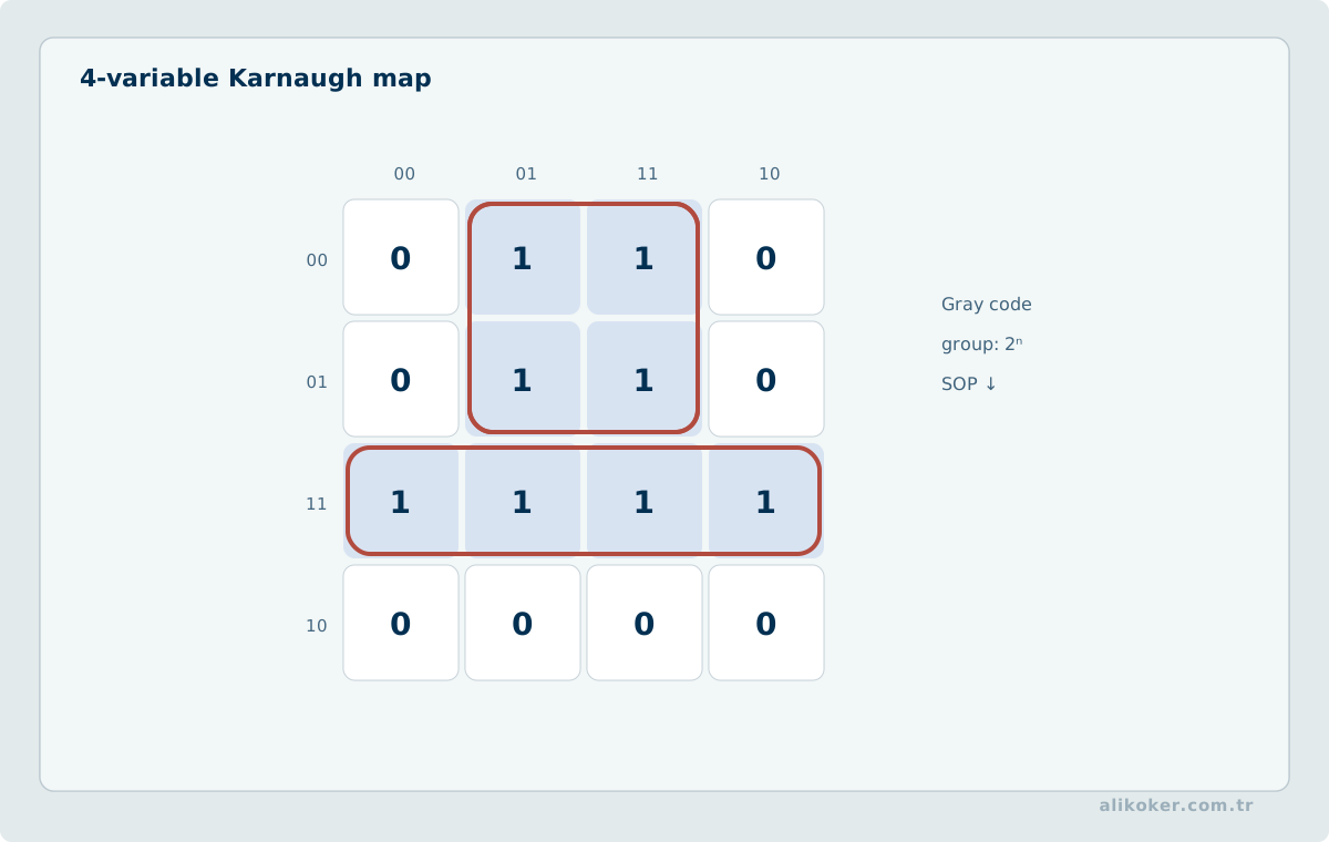
The map contains 2^n cells for n variables. Rows and columns must use Gray ordering, for example:
00 01 11 10rather than ordinary binary order.
Grouping rules
For SOP simplification, group 1 cells in rectangles whose sizes are powers of two:
1, 2, 4, 8, ...Groups may wrap across map edges because the first and last rows/columns are logically adjacent. Larger valid groups remove more variables. Overlap is allowed when it produces a simpler cover.
For POS, group zero cells instead.
Don't-care conditions
Input combinations that cannot occur or whose output is irrelevant may be marked as don't-care. They can be treated as 0 or 1 independently to obtain a simpler circuit, but only when the system specification truly permits either output.
Limits
Karnaugh maps are convenient for small variable counts. Algorithmic minimization and synthesis tools are better for large designs; a K-map is a teaching and manual-design aid rather than a scalable industrial optimizer.
Unit 6: Combinational Circuit Design
Design process
A combinational circuit has outputs determined by current inputs only. A disciplined design process is:
- define input/output meaning,
- form the truth table,
- derive output functions,
- simplify,
- implement and verify.
Half adder
A half adder adds two bits:
S = A XOR B
C = A B
It has no carry input.
Full adder
A full adder adds A, B and carry-in Cin:
S = A XOR B XOR Cin
Cout = AB + ACin + BCin
It can be constructed from two half adders and an OR gate.
Parallel adder
Cascading full adders creates a multi-bit ripple-carry adder. Carry propagates from lower to higher positions, so the worst-case delay grows with word width. Faster architectures reduce carry propagation through lookahead, prefix or related structures.
Subtraction with two's complement
An adder can perform subtraction:
A - B = A + (~B + 1)Hardware often uses a control signal to conditionally complement B and supply the initial carry-in, allowing one adder structure to support addition and subtraction.
Comparators
A magnitude comparator produces relations such as:
A < B
A = B
A > B
Multi-bit comparison proceeds from the most significant unequal position. Cascaded comparator blocks propagate higher-order equality/greater/less information through lower groups.
Unit 7: Encoders and Decoders
Encoder
An encoder maps one-of-many asserted input lines to a compact binary code. A simple encoder assumes only one input is active.
A priority encoder resolves multiple simultaneous active inputs by assigning a defined priority, often also providing a valid indicator.
Decoder
A decoder maps an n-bit code to up to 2^n output lines. For a 2-to-4 decoder, exactly one output corresponds to each binary input combination when enabled.
Enable inputs are useful for cascading decoder blocks and for controlling when outputs participate in a larger circuit.
Decoders can implement Boolean functions by OR-ing the minterm outputs corresponding to desired truth-table rows.
Priority encoders, enable signals, and scalable decoding
A simple encoder assumes that only one input is active. A priority encoder defines which input wins when several inputs are asserted. This makes the circuit suitable for interrupt prioritization and arbitration-like problems.
Decoder enable inputs allow larger decoders to be built hierarchically. The enable path is also part of timing: a logically correct decoded output may still violate a downstream setup requirement if enable and address paths have different delays.
Multiplexers can implement arbitrary Boolean functions by mapping variables to select lines and constants or literals to data inputs. This makes them useful as both routing elements and logic-building blocks.
Unit 8: Multiplexers, Demultiplexers and Three-State Logic
Multiplexer
A multiplexer selects one of several data inputs according to select lines. A 2-to-1 multiplexer implements:
Y = S' I0 + S I1A 4-to-1 multiplexer uses two select bits. Multiplexers can also implement arbitrary Boolean functions by assigning variables to select lines and constants/subexpressions to data inputs.
Demultiplexer
A demultiplexer routes one data input to one selected output. Decoder and demultiplexer structures are closely related but differ in how the data/enable input is interpreted.
Three-state output
A three-state output can be logical 0, logical 1, or high impedance Z. High impedance allows a device to disconnect electrically from a shared line.
Tri-state buses were historically common for board-level and some internal bus structures. Modern FPGA internal routing generally maps logical tri-state descriptions into multiplexer networks, while physical I/O pins can still provide real three-state behavior.
Unit 9: Parity Circuits and the Arithmetic Logic Unit
Parity
Parity adds one redundant bit for simple error detection. With even parity, the total number of 1 bits is even; with odd parity it is odd.
XOR networks naturally generate parity:
P = A XOR B XOR C XOR ...A single parity bit detects any odd number of bit inversions but cannot correct errors and does not detect every even-numbered error pattern.
Arithmetic Logic Unit
An ALU combines arithmetic and logical operations under function-selection controls. Typical operations include:
- addition,
- subtraction,
- AND,
- OR,
- XOR,
- shifts or pass-through operations depending on the design.
The ALU normally also produces status information.
Status flags
Common flags include:
- zero: result is zero,
- sign/negative: typically derived from the most significant result bit for signed interpretation,
- carry: unsigned carry/borrow-related information,
- overflow: signed arithmetic result is not representable,
- parity: parity of a selected result field in architectures that define it.
Carry and signed overflow must not be confused.
Unit 10: Sequential Logic Circuits
State
Unlike a combinational circuit, a sequential circuit's output can depend on both current inputs and stored state. Memory elements therefore become part of the logical model.
Latches
An SR latch can be constructed from cross-coupled NOR or NAND gates. Its set, reset and hold behavior depends on the chosen active-high or active-low implementation. One input combination is forbidden or problematic in the basic form.
A gated latch adds an enable condition. A D latch removes the ambiguous S/R command pair by deriving set/reset behavior from one data input.
Flip-flops
A flip-flop samples according to a clock event rather than being transparent throughout an enable level. Common types include:
- SR,
- D,
- T,
- JK.
A D flip-flop stores the sampled value of D. A T flip-flop toggles when enabled. A JK flip-flop generalizes SR behavior and toggles for the appropriate J/K combination.
Clock edge, setup and hold
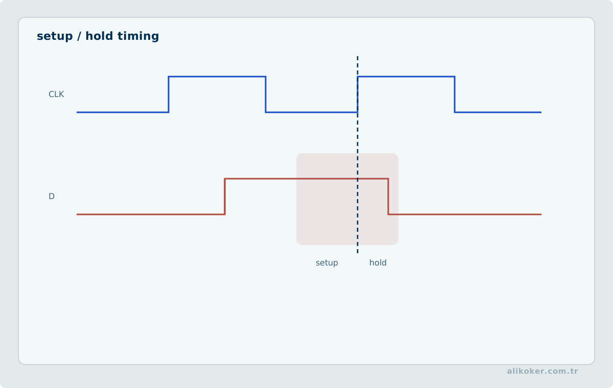
Edge-triggered storage requires input timing around the active clock edge. Setup time is the interval for which data must be stable before the edge; hold time is the interval it must remain stable afterward.
Violating these constraints can lead to metastability. A logical simulation that ignores analog timing does not remove this physical limitation.
Master-slave concept
A traditional master-slave arrangement uses complementary phases/levels of storage elements to obtain edge-like behavior. Modern standard-cell flip-flops can be implemented differently internally, but the model remains useful for understanding why state updates are synchronized.
Unit 11: Synchronous Counter Design
Counters
A counter is a sequential circuit whose states follow a defined sequence. A modulo-m counter cycles through m distinct states.
The minimum number of state bits is:
ceil(log2(m))although unused binary states may exist and should have defined recovery behavior when reliability matters.
Synchronous and ripple counters
In a ripple counter, one flip-flop output clocks another, so transition delay accumulates through the chain. In a synchronous counter, all state flip-flops share a clock and combinational logic determines the next state. Synchronous design is easier to time predictably at higher frequencies.
Decimal and ring counters
A decimal/BCD counter cycles through ten valid states. The six unused four-bit states should be considered in the next-state design rather than assumed impossible forever.
A ring counter circulates a one-hot or patterned bit through a shift register. It uses more flip-flops than a binary counter for the same number of states but can simplify decoding.
Timing
A synchronous design must satisfy propagation, setup, hold and clock-distribution constraints. The logical next-state function may be correct while the physical circuit still fails timing.
Unit 12: Registers and Shift Registers
A register stores a multi-bit word in a set of flip-flops. A load-enable register changes state only when its control is asserted.
Shift registers move data one position per clock. They can support:
- serial-in/serial-out,
- serial-in/parallel-out,
- parallel-in/serial-out,
- parallel-in/parallel-out,
- bidirectional shifting.
They are used in serialization, delay lines, simple sequence generators and data conversion between serial and parallel interfaces.
A universal shift register usually combines hold, left shift, right shift and parallel load under mode controls.
Unit 13: Memory and Programmable Logic
ROM and RAM concepts
ROM-like devices store a mapping from address to data. RAM supports read and write operations. In digital-design terms, a ROM can also implement combinational logic: input variables form an address and stored bits form function outputs.
SRAM stores state in bistable cells and does not need refresh while powered. DRAM stores charge in capacitive cells and requires periodic refresh. Their density, latency and implementation characteristics differ substantially.
Programmable logic
PROM, PLA and PAL structures historically illustrated the idea of programmable product/sum planes. Modern CPLDs and FPGAs generalize programmable logic with configurable logic elements, routing and embedded resources.
An FPGA implementation should be described synchronously and with explicit clock-domain, reset and timing assumptions. HDL syntax is not a software execution sequence; it specifies hardware structure and behavior that synthesis maps to circuitry.
Unit 14: State Machines
State-table model
A finite-state sequential circuit can be represented by:
next_state = f(current_state, input)
output     = g(current_state, input)
for a Mealy model, or:
output = g(current_state)for Moore-style output.
Design steps are typically:
- identify states,
- define transitions,
- form a state diagram/table,
- choose state encoding,
- derive next-state/output logic,
- verify reachable and exceptional states.
State assignment affects logic complexity, switching and implementation. Binary, one-hot and Gray-like encodings have different tradeoffs.
Expanded state tables
An expanded table can include current state, input, next state, outputs and the flip-flop excitation values required by the chosen storage element. For D flip-flops, next-state bits directly become D inputs. For JK or T flip-flops, excitation equations must be derived.
State-machine synthesis and unreachable states
A synchronous finite-state machine separates state storage from next-state and output logic. Moore outputs depend only on state; Mealy outputs can also depend directly on current inputs.
A robust design flow is:
requirements
-> state definition
-> transition table
-> state encoding
-> next-state/output equations
-> timing verification
Unused state encodings should not be ignored automatically. In safety-relevant logic, the design may define a recovery transition from every illegal state to a known safe state.
Counter design follows the same principle. Ripple counters propagate timing through stages, while synchronous counters compute the next state under a common clock and are easier to reason about at higher clock rates.
Overall Framework of the Course
The subjects form a continuous abstraction chain:
number representation
        ↓
Boolean algebra
        ↓
logic gates
        ↓
combinational blocks
        ↓
storage elements
        ↓
registers and counters
        ↓
finite-state machines
        ↓
processor datapaths and control
The important connection is that processor-scale structures are built from the same principles introduced by basic logic gates. Boolean simplification controls combinational cost; timing and state determine sequential correctness; encoding determines how abstract information becomes bits. Digital design is therefore not a collection of unrelated gate symbols but a hierarchy from representation to stateful computation.
Connection to mechanical computation
My examination of a FACIT mechanical calculator provides a historical non-electronic comparison for arithmetic state, carry and digit mechanisms discussed in digital logic.
Clock-domain crossing, metastability, and reset design
Synchronous design becomes unsafe when signals are assumed to share a clock domain without proof. A control bit arriving asynchronously can drive a receiving flip-flop into metastability. Two-stage synchronizers are common for single-bit controls; multi-bit transfers need protocols such as handshakes, Gray-coded counters, or asynchronous FIFOs.
Reset behavior is also a clock-domain problem. Designers must define how reset is asserted and released, especially across unrelated clocks.
CDC and reset-domain analysis complement functional simulation because intermittent hardware failures may never appear in ordinary RTL simulation.
Hazards, Synthesis, and Static Timing
A truth table describes the logical result that a circuit should produce, but physical gates and interconnects do not have zero delay. Two implementations of the same Boolean function can therefore behave differently during transitions.
Hazards
When an input changes, unequal propagation delay through different logic paths can create a transient incorrect pulse. This is a hazard.
logically:        1 -------- 1
physical change:  1 ---0---- 1
A static hazard temporarily changes a value that should have remained constant. A dynamic hazard produces multiple transitions where only one was expected. A synchronous design may tolerate some internal glitches, but the result can become critical when an asynchronous control path or another clock domain samples them.
RTL is not the synthesized circuit
RTL describes intended clocked behavior. Synthesis maps that behavior to gates, multiplexers, registers, and target-technology cells. The same RTL may produce different netlists under different optimization targets or FPGA/ASIC technologies.
Therefore:
RTL simulation
!=
synthesized logic
!=
post-place-and-route timing
Functional simulation answers a logical question; physical timing analysis answers a separate timing question.
Static timing analysis
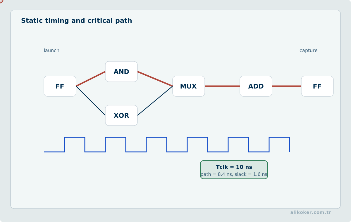
A simplified synchronous timing constraint can be read as:
Tclk >= Tcq + Tcomb + Tsetup + TskewThe source register's clock-to-Q delay, combinational-path delay, destination setup requirement, and clock-distribution difference all participate in the timing budget.
The hold condition is different: new data must not reach the destination before the previous value has been sampled safely. Lowering clock frequency may help a setup violation but does not automatically repair a hold violation.
Timing constraints are design inputs
Without clock periods, input/output delays, and explicit exceptions such as false or multicycle paths, synthesis and timing tools do not know the complete timing contract of the design. A design that "synthesizes successfully" is not therefore proven to operate reliably at the target frequency.
Digital verification should answer three distinct questions:
- Is the logical function correct?
- Are clock-domain and reset boundaries safe?
- Do physical path delays satisfy the timing budget?
Connecting RTL results to hardware reality
A design that passes functional simulation can still fail in hardware because of timing, metastability, or reset-release behavior. Truth tables and RTL simulation are therefore only the first verification layer.
Clock-domain crossings require different techniques for single-bit controls, multi-bit data, and counters. CDC analysis, timing constraints, and post-synthesis reports make the design assumptions explicit. Metastability cannot be eliminated completely; its probability is managed.
FPGA/ASIC examples should identify the target family, clock rate, and relevant primitives. This separates general digital-logic principles from vendor-specific resource behavior.
From Digital Logic to AI Accelerators
An AI accelerator is still a digital circuit. Matrix multiplication, convolution, and attention eventually reduce to Boolean logic, registers, adders, multipliers, multiplexers, control, and memory structures. The connection between digital logic and AI therefore comes from mapping computation to physical circuits, not from the learning theory itself.
A common neural-network primitive is multiply-accumulate:
acc = acc + w * xA layer may repeat this operation millions of times. A general-purpose processor executes it through an instruction stream; a domain-specific accelerator may place many MAC units in parallel and organize dataflow around them. The design problem is not simply to build a faster multiplier, but to feed many arithmetic units efficiently.
Systolic arrays illustrate the idea. Data moves through a regular grid of processing elements; each element performs local multiply-accumulate operations while weights and activations are reused. The basic elements remain familiar:
register
+ combinational arithmetic
+ control
+ local data movement
Bit width directly affects the design. INT8 arithmetic can reduce storage and allow more parallel units than wider floating-point formats, but changes range and numerical error. Saturation, sign handling, rounding, and overflow become system-level properties because they may alter model output.
Activation functions create different hardware costs as well. A function approximable by comparisons and additions is not equivalent to a high-accuracy implementation requiring exponentiation or division. Algorithm and circuit cannot be selected independently when latency, power, or silicon area is constrained.
Memory is often the dominant limitation. If weights repeatedly travel from external memory, arithmetic units may stall and energy cost can be dominated by movement rather than multiplication. Register files, SRAM buffers, banking, and reuse strategies are therefore central to accelerator design.
FPGA inference provides another direct example. Selected model operators can be mapped into fixed data paths and pipelines. The advantage comes from reconfiguring digital hardware around an application-specific flow, not from executing the same instruction stream as a CPU.
Digital logic does not form the mathematical foundation of AI. It forms the implementation layer through which AI computation becomes parallel, bounded-latency, and energy-aware hardware.
From truth tables to timing behaviour
Logical correctness and timing correctness are separate properties of a digital circuit. In combinational logic, outputs depend only on current inputs. Sequential logic also depends on stored state, so a flip-flop, counter, or state machine cannot be fully described by a truth table without clocking and timing assumptions.
Boolean simplification aims to reduce gate count or logic depth without changing the function. Karnaugh-map grouping uses power-of-two groups, with opposite edges treated as adjacent. Larger legal groups often produce simpler expressions, but every required 1 cell still has to be covered.
A half adder combines two bits; a full adder also accepts a carry from the previous position. In a multi-bit ripple-carry adder, carry propagation through successive stages creates the critical delay. More advanced carry structures reduce this path rather than changing the arithmetic definition.
Setup and hold times describe intervals around a clock edge during which a flip-flop input must remain stable. Violating them can create metastability risk. A synchroniser chain can be appropriate for a single control bit crossing clock domains, but synchronising the bits of a multi-bit word independently does not guarantee a coherent transferred word.
For a finite-state machine, state encoding, transition logic, and output logic should be read separately. Moore outputs depend only on state; Mealy outputs can depend on both state and current input. The distinction affects response timing and possible transient output behaviour.
References
- IEEE. IEEE Std 1800-2012 SystemVerilog. IEEE, 2013. Source
- John F. Wakerly. Digital Design: Principles and Practices. Pearson, 2005.
- M. Morris Mano; Michael D. Ciletti. Digital Design. Pearson, 2012.
- Norman P. Jouppi et al. “In-Datacenter Performance Analysis of a Tensor Processing Unit.” Proceedings of ISCA, 2017. https://doi.org/10.1145/3079856.3080246
- Vivienne Sze et al. “Efficient Processing of Deep Neural Networks: A Tutorial and Survey.” Proceedings of the IEEE, 105(12), 2017. https://doi.org/10.1109/JPROC.2017.2761740
